

Key Insights
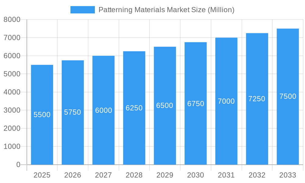
The global Patterning Materials Market is poised for substantial growth, with an estimated market size of $11.44 billion by 2025. The market is projected to expand at a Compound Annual Growth Rate (CAGR) of 11.17% through 2033. This upward trend is significantly driven by the escalating demand for advanced semiconductor devices, fueled by the pervasive adoption of artificial intelligence, 5G networks, the Internet of Things (IoT), and high-performance computing. Key catalysts include ongoing innovations in Integrated Circuits (ICs) and Printed Circuit Boards (PCBs), where precise patterning is essential for device miniaturization and enhanced functionality. The increasing complexity of chip designs necessitates advanced positive photoresists, particularly 248 nm and 193 nm dry resist variants, to achieve superior resolution and yield. Furthermore, the expanding markets for MEMS (Micro-Electro-Mechanical Systems) and NEMS (Nano-Electro-Mechanical Systems) devices, alongside the critical need for advanced memory solutions like DRAM, are major contributors to market expansion. Emerging applications in advanced sensors also present significant opportunities for patterning material suppliers.
Patterning Materials Market Market Size (In Billion)
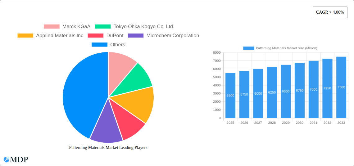
The competitive landscape features prominent global players such as Merck KGaA, Tokyo Ohka Kogyo Co., Ltd., Applied Materials Inc., DuPont, and Shin-Etsu Chemical Co., Ltd., alongside JSR Micro Inc. and Fujifilm Holdings Corporation. These companies are actively investing in research and development to introduce novel patterning materials offering enhanced resolution, sensitivity, and process latitude. Current trends indicate a strong focus on advanced lithography techniques and materials supporting sub-10nm node manufacturing. Geographically, the Asia Pacific region, particularly China, South Korea, and Japan, is anticipated to lead the market due to its concentration of semiconductor manufacturing and R&D investments. North America and Europe also represent significant markets, driven by advanced electronics industries and a growing emphasis on localized semiconductor production. Market restraints include the substantial capital expenditure for advanced lithography equipment, complex regulatory environments for chemical usage, and persistent cost-reduction pressures without performance compromise.
Patterning Materials Market Company Market Share
Patterning Materials Market: Unlocking Innovation in Semiconductor Manufacturing & Beyond (2025-2033)
This comprehensive report delves into the dynamic patterning materials market, a critical enabler for advancements in semiconductors, microelectronics, and beyond. With the global demand for sophisticated electronic devices soaring, the need for high-performance patterning materials has never been greater. This in-depth analysis, covering the study period of 2019–2033, with a base year of 2025 and a forecast period of 2025–2033, provides unparalleled insights into market dynamics, key trends, leading segments, and future opportunities. Explore the intricate landscape of I-line and g-line, Positive 248 nm, Positive 193 nm Dry Resist, TARC, and Other Types, and their pivotal role in applications such as Integrated Circuits and PCBs, MEMS and NEMS Devices, Sensors, Dynamic Random Access Memory, and Other Applications. Discover the strategies of industry giants like Merck KGaA, Tokyo Ohka Kogyo Co Ltd, Applied Materials Inc, DuPont, Microchem Corporation, Shin-Etsu Chemical Co Ltd, JSR Micro Inc, Honeywell Electronic Materials Inc, MacDermid Inc, and Fujifilm Holdings Corporation. This report is an indispensable resource for stakeholders seeking to capitalize on the burgeoning patterning materials market.
Patterning Materials Market Market Dynamics & Concentration
The patterning materials market exhibits a moderately concentrated structure, with a few dominant players holding significant market share, estimated to be around 65% in 2025. Key innovation drivers include the relentless pursuit of miniaturization in semiconductor manufacturing, necessitating the development of materials with higher resolution and sensitivity. Regulatory frameworks, particularly those concerning environmental impact and safety standards, are increasingly influencing material composition and production processes. Product substitutes, while present in niche applications, are largely unable to match the performance characteristics of advanced patterning materials for high-end semiconductor fabrication. End-user trends are characterized by a growing demand for faster, more energy-efficient, and smaller electronic devices, directly impacting the specifications and adoption rates of patterning materials. Mergers and acquisition (M&A) activities have been moderate, with approximately 3-5 significant deals projected annually between 2025 and 2033, aimed at consolidating market position, acquiring novel technologies, and expanding geographical reach. Companies are focusing on strategic alliances and R&D collaborations to maintain a competitive edge.
Patterning Materials Market Industry Trends & Analysis
The patterning materials market is poised for robust growth, driven by the insatiable global demand for advanced electronic components. The market is projected to witness a Compound Annual Growth Rate (CAGR) of approximately 7.5% from 2025 to 2033. This expansion is fundamentally fueled by the continuous evolution of the semiconductor industry, with an increasing focus on higher transistor densities and more complex chip architectures. Technological disruptions, such as the advent of Extreme Ultraviolet (EUV) lithography, are profoundly reshaping the demand for specialized patterning materials like advanced photoresists and ancillary chemicals. While the initial investment in EUV infrastructure is substantial, its capacity to enable sub-10nm node fabrication makes it a critical trend. Consumer preferences are increasingly leaning towards smaller, more powerful, and interconnected devices, including smartphones, wearables, and advanced automotive electronics, all of which rely heavily on sophisticated semiconductor manufacturing processes. The competitive dynamics within the market are characterized by intense R&D investments, strategic partnerships between material suppliers and foundries, and a constant drive for cost optimization without compromising performance. Market penetration of advanced patterning materials is expected to reach over 85% in the high-end semiconductor segment by 2033. The ongoing development of novel materials with enhanced etch resistance, reduced defectivity, and improved process windows are key areas of focus. Furthermore, the growing adoption of 3D integrated circuits and heterogeneous integration technologies are creating new avenues for specialized patterning solutions. The circular economy principles are also beginning to influence material selection, with a growing emphasis on sustainable sourcing and waste reduction in the production of patterning materials.
Leading Markets & Segments in Patterning Materials Market
The patterning materials market is dominated by the Integrated Circuits and PCBs application segment, which is expected to account for a substantial market share of over 50% by 2025. This dominance is primarily driven by the ever-increasing demand for more powerful and complex processors, memory chips, and printed circuit boards across consumer electronics, telecommunications, and data centers.
Key Drivers for Dominance in Integrated Circuits and PCBs:
- Economic Policies: Government incentives and favorable trade policies supporting domestic semiconductor manufacturing are bolstering demand for advanced patterning materials in key regions like Asia-Pacific and North America.
- Infrastructure Development: Significant investments in fab construction and expansion globally directly translate to higher consumption of patterning materials.
- Technological Advancements: The relentless march towards smaller process nodes (e.g., 7nm, 5nm, and below) necessitates the use of highly specialized and advanced patterning materials.
Within the Type segment, Positive 193 nm Dry Resist is anticipated to lead, driven by its widespread adoption in current mainstream lithography processes for advanced ICs. However, the emergence of Positive 248 nm materials for specific applications and the ongoing research in Other Types, including EUV-related materials, represent significant growth areas.
Dominance Analysis of Key Segments:
- Application: Integrated Circuits and PCBs: The sheer volume of semiconductor production for everyday devices, coupled with the high-value nature of advanced ICs, makes this segment the undisputed leader. The continuous innovation cycle in this area ensures a sustained demand for cutting-edge patterning solutions.
- Type: Positive 193 nm Dry Resist: This material type has become the workhorse for many advanced lithography processes due to its balance of performance, cost-effectiveness, and maturity. Its compatibility with existing fab infrastructure ensures continued widespread adoption.
- Region: Asia-Pacific: This region is the global hub for semiconductor manufacturing, housing a significant majority of foundries and assembly and testing facilities. Favorable manufacturing costs, government support, and a vast consumer market drive the demand for patterning materials. Countries like Taiwan, South Korea, and China are at the forefront of this trend.
Other significant segments contributing to market growth include MEMS and NEMS Devices and Sensors, driven by the proliferation of IoT devices and advanced instrumentation. While Dynamic Random Access Memory is a mature segment, its continued importance in computing ensures a steady demand for patterning materials.
Patterning Materials Market Product Developments
Product developments in the patterning materials market are characterized by a relentless focus on enhancing resolution, reducing defectivity, and improving process efficiency for next-generation semiconductor manufacturing. Innovations are centered around advanced photoresist formulations, including novel polymers and sensitizers, designed to meet the stringent requirements of sub-10nm lithography. The development of environmentally friendly and sustainable patterning solutions is also gaining traction, reflecting industry-wide ESG initiatives. Companies are also developing ancillary materials like anti-reflective coatings (ARCs) and developers that offer synergistic performance benefits with advanced photoresists, providing a competitive advantage in terms of process control and yield enhancement.
Key Drivers of Patterning Materials Market Growth
The patterning materials market is propelled by several key drivers. Technologically, the incessant demand for smaller, faster, and more power-efficient electronic devices, particularly driven by AI, 5G, and IoT, necessitates advancements in lithography and, consequently, patterning materials. Economic factors such as increasing global semiconductor investments in new fabs and R&D funding fuel market expansion. Regulatory advancements, while sometimes presenting challenges, also drive innovation towards safer and more sustainable material compositions. For instance, the push for stricter environmental regulations is spurring the development of new chemistries with lower volatile organic compound (VOC) emissions.
Challenges in the Patterning Materials Market Market
Despite its robust growth trajectory, the patterning materials market faces several challenges. High R&D costs and long development cycles for new materials, especially for cutting-edge technologies like EUV lithography, pose a significant barrier. Supply chain complexities and potential geopolitical disruptions can impact the availability and pricing of critical raw materials. Stringent quality control requirements and the high cost of qualification for new materials by semiconductor manufacturers also present hurdles. Intense competition among established players and emerging entrants can lead to price pressures, impacting profit margins. Furthermore, the rapid pace of technological change means that materials developed for one generation of chip manufacturing may become obsolete quickly.
Emerging Opportunities in Patterning Materials Market
Emerging opportunities in the patterning materials market lie in the rapid growth of specialized applications. The increasing adoption of advanced packaging technologies, such as 3D ICs and chiplets, is creating demand for novel patterning solutions for interconnections and wafer-level processing. The expansion of the MEMS and NEMS devices market, driven by applications in automotive, healthcare, and consumer electronics, presents another significant opportunity for tailored patterning materials. Furthermore, the development of materials for next-generation lithography techniques, including directed self-assembly (DSA) and multi-beam lithography, offers substantial long-term growth potential. Strategic partnerships between material suppliers and leading semiconductor manufacturers are crucial for co-developing and accelerating the adoption of these next-generation solutions.
Leading Players in the Patterning Materials Market Sector
- Merck KGaA
- Tokyo Ohka Kogyo Co Ltd
- Applied Materials Inc
- DuPont
- Microchem Corporation
- Shin-Etsu Chemical Co Ltd
- JSR Micro Inc
- Honeywell Electronic Materials Inc
- MacDermid Inc
- Fujifilm Holdings Corporation
Key Milestones in Patterning Materials Market Industry
- 2019: Introduction of advanced anti-reflective coatings (ARCs) to improve lithographic resolution for sub-20nm nodes.
- 2020: Increased R&D focus on materials for EUV lithography, with significant breakthroughs in photoresist sensitivity and etch resistance.
- 2021: Several key players announced strategic partnerships to accelerate the development of next-generation patterning materials.
- 2022: Growing emphasis on sustainable material development, with companies highlighting reduced VOC emissions in their product portfolios.
- 2023: Significant investments in advanced packaging solutions are driving demand for specialized patterning materials for 3D integration.
- 2024: Emergence of new material chemistries designed for enhanced performance in dry lithography processes.
Strategic Outlook for Patterning Materials Market Market
The strategic outlook for the patterning materials market is highly positive, driven by sustained innovation and expanding applications. Key growth accelerators include the ongoing miniaturization of semiconductor nodes, the burgeoning demand for advanced packaging solutions, and the increasing adoption of MEMS and NEMS devices. Companies that can effectively navigate the complexities of EUV lithography material development and provide cost-effective, high-performance solutions will be well-positioned for success. Strategic collaborations with leading semiconductor manufacturers and a focus on sustainability will be crucial for long-term market leadership and capturing emerging opportunities. The market is expected to witness continued consolidation and investment in advanced R&D to maintain a competitive edge.
Patterning Materials Market Segmentation
-
1. Type
- 1.1. I-line and g-line
- 1.2. Positive 248 nm
- 1.3. Positive 193 nm Dry Resist
- 1.4. TARC
- 1.5. Other Types
-
2. Applications
- 2.1. Integrated Circuits and PCBs
- 2.2. MEMS and NEMS Devices
- 2.3. Sensors
- 2.4. Dynamic Random Access Memory
- 2.5. Other Applications
Patterning Materials Market Segmentation By Geography
-
1. Asia Pacific
- 1.1. China
- 1.2. India
- 1.3. Japan
- 1.4. South Korea
- 1.5. Rest of Asia Pacific
-
2. North America
- 2.1. United States
- 2.2. Canada
- 2.3. Mexico
-
3. Europe
- 3.1. Germany
- 3.2. United Kingdom
- 3.3. France
- 3.4. Italy
- 3.5. Rest of Europe
- 4. Rest of the World
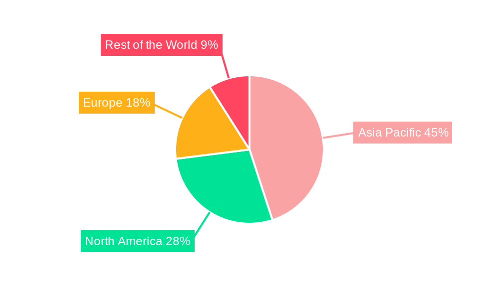
Patterning Materials Market Regional Market Share
Geographic Coverage of Patterning Materials Market
Patterning Materials Market REPORT HIGHLIGHTS
| Aspects | Details |
|---|---|
| Study Period | 2020-2034 |
| Base Year | 2025 |
| Estimated Year | 2026 |
| Forecast Period | 2026-2034 |
| Historical Period | 2020-2025 |
| Growth Rate | CAGR of 11.17% from 2020-2034 |
| Segmentation |
|
Table of Contents
- 1. Introduction
- 1.1. Research Scope
- 1.2. Market Segmentation
- 1.3. Research Objective
- 1.4. Definitions and Assumptions
- 2. Executive Summary
- 2.1. Market Snapshot
- 3. Market Dynamics
- 3.1. Market Drivers
- 3.2. Market Restrains
- 3.3. Market Trends
- 3.4. Market Opportunities
- 4. Market Factor Analysis
- 4.1. Porters Five Forces
- 4.1.1. Bargaining Power of Suppliers
- 4.1.2. Bargaining Power of Buyers
- 4.1.3. Threat of New Entrants
- 4.1.4. Threat of Substitutes
- 4.1.5. Competitive Rivalry
- 4.2. PESTEL analysis
- 4.3. BCG Analysis
- 4.3.1. Stars (High Growth, High Market Share)
- 4.3.2. Cash Cows (Low Growth, High Market Share)
- 4.3.3. Question Mark (High Growth, Low Market Share)
- 4.3.4. Dogs (Low Growth, Low Market Share)
- 4.4. Ansoff Matrix Analysis
- 4.5. Supply Chain Analysis
- 4.6. Regulatory Landscape
- 4.7. Current Market Potential and Opportunity Assessment (TAM–SAM–SOM Framework)
- 4.8. MDP Analyst Note
- 4.1. Porters Five Forces
- 5. Market Analysis, Insights and Forecast 2021-2033
- 5.1. Market Analysis, Insights and Forecast - by Type
- 5.1.1. I-line and g-line
- 5.1.2. Positive 248 nm
- 5.1.3. Positive 193 nm Dry Resist
- 5.1.4. TARC
- 5.1.5. Other Types
- 5.2. Market Analysis, Insights and Forecast - by Applications
- 5.2.1. Integrated Circuits and PCBs
- 5.2.2. MEMS and NEMS Devices
- 5.2.3. Sensors
- 5.2.4. Dynamic Random Access Memory
- 5.2.5. Other Applications
- 5.3. Market Analysis, Insights and Forecast - by Region
- 5.3.1. Asia Pacific
- 5.3.2. North America
- 5.3.3. Europe
- 5.3.4. Rest of the World
- 5.1. Market Analysis, Insights and Forecast - by Type
- 6. Global Patterning Materials Market Analysis, Insights and Forecast, 2021-2033
- 6.1. Market Analysis, Insights and Forecast - by Type
- 6.1.1. I-line and g-line
- 6.1.2. Positive 248 nm
- 6.1.3. Positive 193 nm Dry Resist
- 6.1.4. TARC
- 6.1.5. Other Types
- 6.2. Market Analysis, Insights and Forecast - by Applications
- 6.2.1. Integrated Circuits and PCBs
- 6.2.2. MEMS and NEMS Devices
- 6.2.3. Sensors
- 6.2.4. Dynamic Random Access Memory
- 6.2.5. Other Applications
- 6.1. Market Analysis, Insights and Forecast - by Type
- 7. Asia Pacific Patterning Materials Market Analysis, Insights and Forecast, 2020-2032
- 7.1. Market Analysis, Insights and Forecast - by Type
- 7.1.1. I-line and g-line
- 7.1.2. Positive 248 nm
- 7.1.3. Positive 193 nm Dry Resist
- 7.1.4. TARC
- 7.1.5. Other Types
- 7.2. Market Analysis, Insights and Forecast - by Applications
- 7.2.1. Integrated Circuits and PCBs
- 7.2.2. MEMS and NEMS Devices
- 7.2.3. Sensors
- 7.2.4. Dynamic Random Access Memory
- 7.2.5. Other Applications
- 7.1. Market Analysis, Insights and Forecast - by Type
- 8. North America Patterning Materials Market Analysis, Insights and Forecast, 2020-2032
- 8.1. Market Analysis, Insights and Forecast - by Type
- 8.1.1. I-line and g-line
- 8.1.2. Positive 248 nm
- 8.1.3. Positive 193 nm Dry Resist
- 8.1.4. TARC
- 8.1.5. Other Types
- 8.2. Market Analysis, Insights and Forecast - by Applications
- 8.2.1. Integrated Circuits and PCBs
- 8.2.2. MEMS and NEMS Devices
- 8.2.3. Sensors
- 8.2.4. Dynamic Random Access Memory
- 8.2.5. Other Applications
- 8.1. Market Analysis, Insights and Forecast - by Type
- 9. Europe Patterning Materials Market Analysis, Insights and Forecast, 2020-2032
- 9.1. Market Analysis, Insights and Forecast - by Type
- 9.1.1. I-line and g-line
- 9.1.2. Positive 248 nm
- 9.1.3. Positive 193 nm Dry Resist
- 9.1.4. TARC
- 9.1.5. Other Types
- 9.2. Market Analysis, Insights and Forecast - by Applications
- 9.2.1. Integrated Circuits and PCBs
- 9.2.2. MEMS and NEMS Devices
- 9.2.3. Sensors
- 9.2.4. Dynamic Random Access Memory
- 9.2.5. Other Applications
- 9.1. Market Analysis, Insights and Forecast - by Type
- 10. Rest of the World Patterning Materials Market Analysis, Insights and Forecast, 2020-2032
- 10.1. Market Analysis, Insights and Forecast - by Type
- 10.1.1. I-line and g-line
- 10.1.2. Positive 248 nm
- 10.1.3. Positive 193 nm Dry Resist
- 10.1.4. TARC
- 10.1.5. Other Types
- 10.2. Market Analysis, Insights and Forecast - by Applications
- 10.2.1. Integrated Circuits and PCBs
- 10.2.2. MEMS and NEMS Devices
- 10.2.3. Sensors
- 10.2.4. Dynamic Random Access Memory
- 10.2.5. Other Applications
- 10.1. Market Analysis, Insights and Forecast - by Type
- 11. Competitive Analysis
- 11.1. Company Profiles
- 11.1.1 Merck KGaA
- 11.1.1.1. Company Overview
- 11.1.1.2. Products
- 11.1.1.3. Company Financials
- 11.1.1.4. SWOT Analysis
- 11.1.2 Tokyo Ohka Kogyo Co Ltd
- 11.1.2.1. Company Overview
- 11.1.2.2. Products
- 11.1.2.3. Company Financials
- 11.1.2.4. SWOT Analysis
- 11.1.3 Applied Materials Inc
- 11.1.3.1. Company Overview
- 11.1.3.2. Products
- 11.1.3.3. Company Financials
- 11.1.3.4. SWOT Analysis
- 11.1.4 DuPont
- 11.1.4.1. Company Overview
- 11.1.4.2. Products
- 11.1.4.3. Company Financials
- 11.1.4.4. SWOT Analysis
- 11.1.5 Microchem Corporation
- 11.1.5.1. Company Overview
- 11.1.5.2. Products
- 11.1.5.3. Company Financials
- 11.1.5.4. SWOT Analysis
- 11.1.6 Shin-Etsu Chemical Co Ltd
- 11.1.6.1. Company Overview
- 11.1.6.2. Products
- 11.1.6.3. Company Financials
- 11.1.6.4. SWOT Analysis
- 11.1.7 JSR Micro Inc
- 11.1.7.1. Company Overview
- 11.1.7.2. Products
- 11.1.7.3. Company Financials
- 11.1.7.4. SWOT Analysis
- 11.1.8 Honeywell Electronic Materials Inc
- 11.1.8.1. Company Overview
- 11.1.8.2. Products
- 11.1.8.3. Company Financials
- 11.1.8.4. SWOT Analysis
- 11.1.9 MacDermid Inc
- 11.1.9.1. Company Overview
- 11.1.9.2. Products
- 11.1.9.3. Company Financials
- 11.1.9.4. SWOT Analysis
- 11.1.10 Fujifilm Holdings Corporation
- 11.1.10.1. Company Overview
- 11.1.10.2. Products
- 11.1.10.3. Company Financials
- 11.1.10.4. SWOT Analysis
- 11.1.1 Merck KGaA
- 11.2. Market Entropy
- 11.2.1 Company's Key Areas Served
- 11.2.2 Recent Developments
- 11.3. Company Market Share Analysis 2025
- 11.3.1 Top 5 Companies Market Share Analysis
- 11.3.2 Top 3 Companies Market Share Analysis
- 11.4. List of Potential Customers
- 12. Research Methodology
List of Figures
- Figure 1: Global Patterning Materials Market Revenue Breakdown (billion, %) by Region 2025 & 2033
- Figure 2: Global Patterning Materials Market Volume Breakdown (K Tons, %) by Region 2025 & 2033
- Figure 3: Asia Pacific Patterning Materials Market Revenue (billion), by Type 2025 & 2033
- Figure 4: Asia Pacific Patterning Materials Market Volume (K Tons), by Type 2025 & 2033
- Figure 5: Asia Pacific Patterning Materials Market Revenue Share (%), by Type 2025 & 2033
- Figure 6: Asia Pacific Patterning Materials Market Volume Share (%), by Type 2025 & 2033
- Figure 7: Asia Pacific Patterning Materials Market Revenue (billion), by Applications 2025 & 2033
- Figure 8: Asia Pacific Patterning Materials Market Volume (K Tons), by Applications 2025 & 2033
- Figure 9: Asia Pacific Patterning Materials Market Revenue Share (%), by Applications 2025 & 2033
- Figure 10: Asia Pacific Patterning Materials Market Volume Share (%), by Applications 2025 & 2033
- Figure 11: Asia Pacific Patterning Materials Market Revenue (billion), by Country 2025 & 2033
- Figure 12: Asia Pacific Patterning Materials Market Volume (K Tons), by Country 2025 & 2033
- Figure 13: Asia Pacific Patterning Materials Market Revenue Share (%), by Country 2025 & 2033
- Figure 14: Asia Pacific Patterning Materials Market Volume Share (%), by Country 2025 & 2033
- Figure 15: North America Patterning Materials Market Revenue (billion), by Type 2025 & 2033
- Figure 16: North America Patterning Materials Market Volume (K Tons), by Type 2025 & 2033
- Figure 17: North America Patterning Materials Market Revenue Share (%), by Type 2025 & 2033
- Figure 18: North America Patterning Materials Market Volume Share (%), by Type 2025 & 2033
- Figure 19: North America Patterning Materials Market Revenue (billion), by Applications 2025 & 2033
- Figure 20: North America Patterning Materials Market Volume (K Tons), by Applications 2025 & 2033
- Figure 21: North America Patterning Materials Market Revenue Share (%), by Applications 2025 & 2033
- Figure 22: North America Patterning Materials Market Volume Share (%), by Applications 2025 & 2033
- Figure 23: North America Patterning Materials Market Revenue (billion), by Country 2025 & 2033
- Figure 24: North America Patterning Materials Market Volume (K Tons), by Country 2025 & 2033
- Figure 25: North America Patterning Materials Market Revenue Share (%), by Country 2025 & 2033
- Figure 26: North America Patterning Materials Market Volume Share (%), by Country 2025 & 2033
- Figure 27: Europe Patterning Materials Market Revenue (billion), by Type 2025 & 2033
- Figure 28: Europe Patterning Materials Market Volume (K Tons), by Type 2025 & 2033
- Figure 29: Europe Patterning Materials Market Revenue Share (%), by Type 2025 & 2033
- Figure 30: Europe Patterning Materials Market Volume Share (%), by Type 2025 & 2033
- Figure 31: Europe Patterning Materials Market Revenue (billion), by Applications 2025 & 2033
- Figure 32: Europe Patterning Materials Market Volume (K Tons), by Applications 2025 & 2033
- Figure 33: Europe Patterning Materials Market Revenue Share (%), by Applications 2025 & 2033
- Figure 34: Europe Patterning Materials Market Volume Share (%), by Applications 2025 & 2033
- Figure 35: Europe Patterning Materials Market Revenue (billion), by Country 2025 & 2033
- Figure 36: Europe Patterning Materials Market Volume (K Tons), by Country 2025 & 2033
- Figure 37: Europe Patterning Materials Market Revenue Share (%), by Country 2025 & 2033
- Figure 38: Europe Patterning Materials Market Volume Share (%), by Country 2025 & 2033
- Figure 39: Rest of the World Patterning Materials Market Revenue (billion), by Type 2025 & 2033
- Figure 40: Rest of the World Patterning Materials Market Volume (K Tons), by Type 2025 & 2033
- Figure 41: Rest of the World Patterning Materials Market Revenue Share (%), by Type 2025 & 2033
- Figure 42: Rest of the World Patterning Materials Market Volume Share (%), by Type 2025 & 2033
- Figure 43: Rest of the World Patterning Materials Market Revenue (billion), by Applications 2025 & 2033
- Figure 44: Rest of the World Patterning Materials Market Volume (K Tons), by Applications 2025 & 2033
- Figure 45: Rest of the World Patterning Materials Market Revenue Share (%), by Applications 2025 & 2033
- Figure 46: Rest of the World Patterning Materials Market Volume Share (%), by Applications 2025 & 2033
- Figure 47: Rest of the World Patterning Materials Market Revenue (billion), by Country 2025 & 2033
- Figure 48: Rest of the World Patterning Materials Market Volume (K Tons), by Country 2025 & 2033
- Figure 49: Rest of the World Patterning Materials Market Revenue Share (%), by Country 2025 & 2033
- Figure 50: Rest of the World Patterning Materials Market Volume Share (%), by Country 2025 & 2033
List of Tables
- Table 1: Global Patterning Materials Market Revenue billion Forecast, by Type 2020 & 2033
- Table 2: Global Patterning Materials Market Volume K Tons Forecast, by Type 2020 & 2033
- Table 3: Global Patterning Materials Market Revenue billion Forecast, by Applications 2020 & 2033
- Table 4: Global Patterning Materials Market Volume K Tons Forecast, by Applications 2020 & 2033
- Table 5: Global Patterning Materials Market Revenue billion Forecast, by Region 2020 & 2033
- Table 6: Global Patterning Materials Market Volume K Tons Forecast, by Region 2020 & 2033
- Table 7: Global Patterning Materials Market Revenue billion Forecast, by Type 2020 & 2033
- Table 8: Global Patterning Materials Market Volume K Tons Forecast, by Type 2020 & 2033
- Table 9: Global Patterning Materials Market Revenue billion Forecast, by Applications 2020 & 2033
- Table 10: Global Patterning Materials Market Volume K Tons Forecast, by Applications 2020 & 2033
- Table 11: Global Patterning Materials Market Revenue billion Forecast, by Country 2020 & 2033
- Table 12: Global Patterning Materials Market Volume K Tons Forecast, by Country 2020 & 2033
- Table 13: China Patterning Materials Market Revenue (billion) Forecast, by Application 2020 & 2033
- Table 14: China Patterning Materials Market Volume (K Tons) Forecast, by Application 2020 & 2033
- Table 15: India Patterning Materials Market Revenue (billion) Forecast, by Application 2020 & 2033
- Table 16: India Patterning Materials Market Volume (K Tons) Forecast, by Application 2020 & 2033
- Table 17: Japan Patterning Materials Market Revenue (billion) Forecast, by Application 2020 & 2033
- Table 18: Japan Patterning Materials Market Volume (K Tons) Forecast, by Application 2020 & 2033
- Table 19: South Korea Patterning Materials Market Revenue (billion) Forecast, by Application 2020 & 2033
- Table 20: South Korea Patterning Materials Market Volume (K Tons) Forecast, by Application 2020 & 2033
- Table 21: Rest of Asia Pacific Patterning Materials Market Revenue (billion) Forecast, by Application 2020 & 2033
- Table 22: Rest of Asia Pacific Patterning Materials Market Volume (K Tons) Forecast, by Application 2020 & 2033
- Table 23: Global Patterning Materials Market Revenue billion Forecast, by Type 2020 & 2033
- Table 24: Global Patterning Materials Market Volume K Tons Forecast, by Type 2020 & 2033
- Table 25: Global Patterning Materials Market Revenue billion Forecast, by Applications 2020 & 2033
- Table 26: Global Patterning Materials Market Volume K Tons Forecast, by Applications 2020 & 2033
- Table 27: Global Patterning Materials Market Revenue billion Forecast, by Country 2020 & 2033
- Table 28: Global Patterning Materials Market Volume K Tons Forecast, by Country 2020 & 2033
- Table 29: United States Patterning Materials Market Revenue (billion) Forecast, by Application 2020 & 2033
- Table 30: United States Patterning Materials Market Volume (K Tons) Forecast, by Application 2020 & 2033
- Table 31: Canada Patterning Materials Market Revenue (billion) Forecast, by Application 2020 & 2033
- Table 32: Canada Patterning Materials Market Volume (K Tons) Forecast, by Application 2020 & 2033
- Table 33: Mexico Patterning Materials Market Revenue (billion) Forecast, by Application 2020 & 2033
- Table 34: Mexico Patterning Materials Market Volume (K Tons) Forecast, by Application 2020 & 2033
- Table 35: Global Patterning Materials Market Revenue billion Forecast, by Type 2020 & 2033
- Table 36: Global Patterning Materials Market Volume K Tons Forecast, by Type 2020 & 2033
- Table 37: Global Patterning Materials Market Revenue billion Forecast, by Applications 2020 & 2033
- Table 38: Global Patterning Materials Market Volume K Tons Forecast, by Applications 2020 & 2033
- Table 39: Global Patterning Materials Market Revenue billion Forecast, by Country 2020 & 2033
- Table 40: Global Patterning Materials Market Volume K Tons Forecast, by Country 2020 & 2033
- Table 41: Germany Patterning Materials Market Revenue (billion) Forecast, by Application 2020 & 2033
- Table 42: Germany Patterning Materials Market Volume (K Tons) Forecast, by Application 2020 & 2033
- Table 43: United Kingdom Patterning Materials Market Revenue (billion) Forecast, by Application 2020 & 2033
- Table 44: United Kingdom Patterning Materials Market Volume (K Tons) Forecast, by Application 2020 & 2033
- Table 45: France Patterning Materials Market Revenue (billion) Forecast, by Application 2020 & 2033
- Table 46: France Patterning Materials Market Volume (K Tons) Forecast, by Application 2020 & 2033
- Table 47: Italy Patterning Materials Market Revenue (billion) Forecast, by Application 2020 & 2033
- Table 48: Italy Patterning Materials Market Volume (K Tons) Forecast, by Application 2020 & 2033
- Table 49: Rest of Europe Patterning Materials Market Revenue (billion) Forecast, by Application 2020 & 2033
- Table 50: Rest of Europe Patterning Materials Market Volume (K Tons) Forecast, by Application 2020 & 2033
- Table 51: Global Patterning Materials Market Revenue billion Forecast, by Type 2020 & 2033
- Table 52: Global Patterning Materials Market Volume K Tons Forecast, by Type 2020 & 2033
- Table 53: Global Patterning Materials Market Revenue billion Forecast, by Applications 2020 & 2033
- Table 54: Global Patterning Materials Market Volume K Tons Forecast, by Applications 2020 & 2033
- Table 55: Global Patterning Materials Market Revenue billion Forecast, by Country 2020 & 2033
- Table 56: Global Patterning Materials Market Volume K Tons Forecast, by Country 2020 & 2033
Frequently Asked Questions
1. What is the projected Compound Annual Growth Rate (CAGR) of the Patterning Materials Market?
The projected CAGR is approximately 11.17%.
2. Which companies are prominent players in the Patterning Materials Market?
Key companies in the market include Merck KGaA, Tokyo Ohka Kogyo Co Ltd, Applied Materials Inc, DuPont, Microchem Corporation, Shin-Etsu Chemical Co Ltd, JSR Micro Inc, Honeywell Electronic Materials Inc, MacDermid Inc, Fujifilm Holdings Corporation.
3. What are the main segments of the Patterning Materials Market?
The market segments include Type, Applications.
4. Can you provide details about the market size?
The market size is estimated to be USD 11.44 billion as of 2022.
5. What are some drivers contributing to market growth?
; Increasing Applications for Electronics; Growing Demand from the Automobile Industry.
6. What are the notable trends driving market growth?
Growing Demand from the Electronics Industry.
7. Are there any restraints impacting market growth?
; Impact of COVID-19; Other Restraints.
8. Can you provide examples of recent developments in the market?
N/A
9. What pricing options are available for accessing the report?
Pricing options include single-user, multi-user, and enterprise licenses priced at USD 4750, USD 5250, and USD 8750 respectively.
10. Is the market size provided in terms of value or volume?
The market size is provided in terms of value, measured in billion and volume, measured in K Tons.
11. Are there any specific market keywords associated with the report?
Yes, the market keyword associated with the report is "Patterning Materials Market," which aids in identifying and referencing the specific market segment covered.
12. How do I determine which pricing option suits my needs best?
The pricing options vary based on user requirements and access needs. Individual users may opt for single-user licenses, while businesses requiring broader access may choose multi-user or enterprise licenses for cost-effective access to the report.
13. Are there any additional resources or data provided in the Patterning Materials Market report?
While the report offers comprehensive insights, it's advisable to review the specific contents or supplementary materials provided to ascertain if additional resources or data are available.
14. How can I stay updated on further developments or reports in the Patterning Materials Market?
To stay informed about further developments, trends, and reports in the Patterning Materials Market, consider subscribing to industry newsletters, following relevant companies and organizations, or regularly checking reputable industry news sources and publications.
Methodology
Step 1 - Identification of Relevant Samples Size from Population Database


Step 2 - Approaches for Defining Global Market Size (Value, Volume* & Price*)

Note*: In applicable scenarios
Step 3 - Data Sources
Primary Research
- Web Analytics
- Survey Reports
- Research Institute
- Latest Research Reports
- Opinion Leaders
Secondary Research
- Annual Reports
- White Paper
- Latest Press Release
- Industry Association
- Paid Database
- Investor Presentations

Step 4 - Data Triangulation
Involves using different sources of information in order to increase the validity of a study
These sources are likely to be stakeholders in a program - participants, other researchers, program staff, other community members, and so on.
Then we put all data in single framework & apply various statistical tools to find out the dynamic on the market.
During the analysis stage, feedback from the stakeholder groups would be compared to determine areas of agreement as well as areas of divergence