

Key Insights
The global Semiconductor Packaging and Test (OSAT) market is poised for significant expansion, projected to reach an estimated $10.9 billion in 2025 with a robust Compound Annual Growth Rate (CAGR) of 9.16% through 2033. This remarkable growth is underpinned by several powerful drivers, primarily the escalating demand for advanced electronics across diverse sectors. The proliferation of 5G technology, the rapid adoption of artificial intelligence (AI) and machine learning (ML) in various applications, and the continuous innovation in the Internet of Things (IoT) are all fueling the need for sophisticated semiconductor packaging solutions. Furthermore, the increasing complexity of integrated circuits (ICs) necessitates highly specialized packaging services to ensure optimal performance, reliability, and miniaturization. The automotive industry's shift towards electric and autonomous vehicles, along with the surging demand for high-performance computing (HPC) for data centers and cloud infrastructure, also contributes significantly to market expansion.
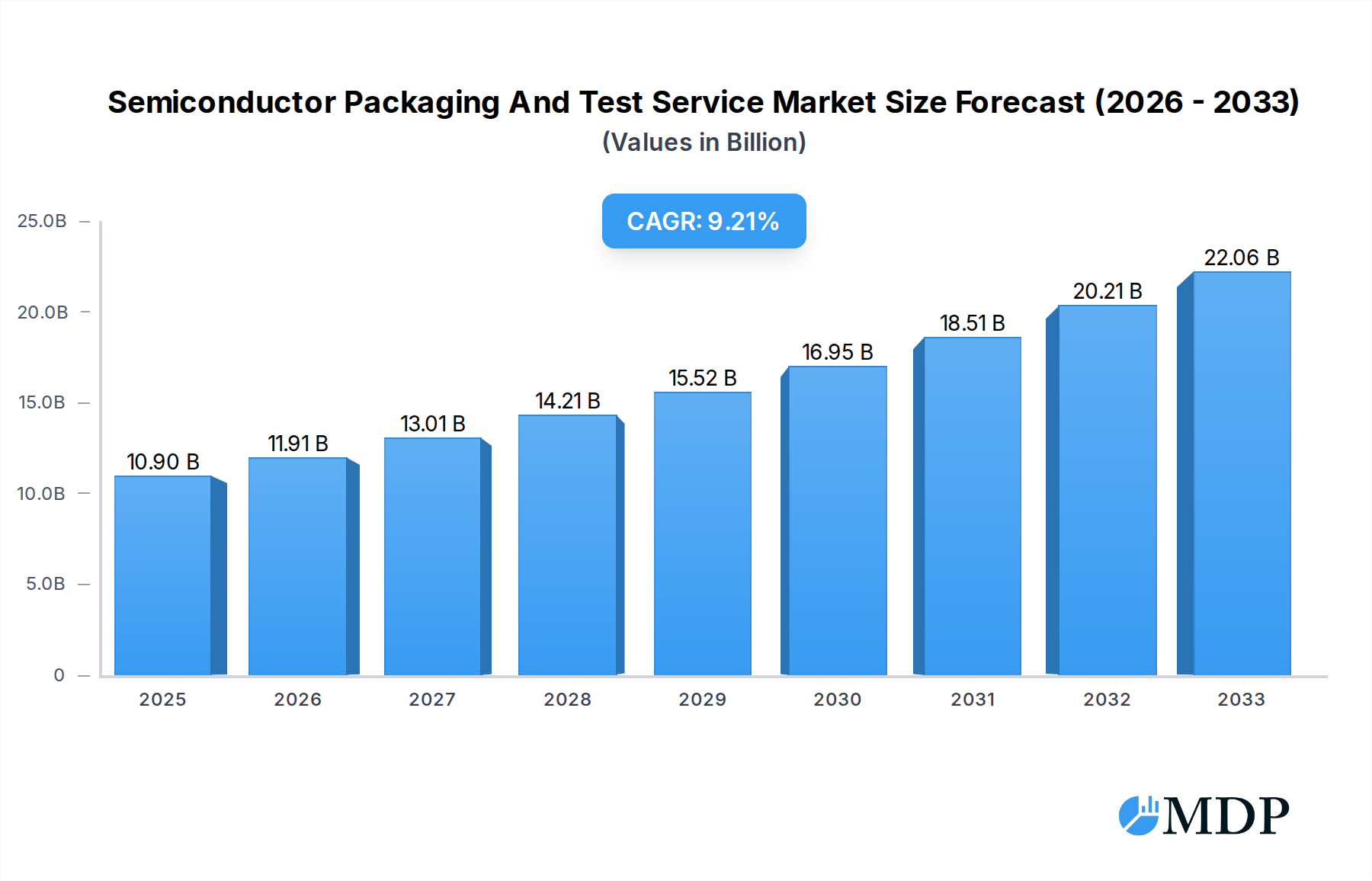
Semiconductor Packaging And Test Service Market Size (In Billion)
Key trends shaping the Semiconductor Packaging and Test Service market include the growing adoption of advanced packaging techniques such as fan-out wafer-level packaging (FOWLP), 2.5D and 3D integration, and heterogeneous integration. These technologies enable higher density, improved performance, and reduced power consumption, crucial for next-generation devices. The market also witnesses a rising focus on miniaturization and power efficiency, driven by the proliferation of wearable devices and portable electronics. Emerging applications in areas like augmented reality (AR) and virtual reality (VR) further propel innovation in packaging solutions. While the market exhibits strong growth, restraints such as rising raw material costs, particularly for advanced packaging substrates and specialized chemicals, and the inherent complexity of semiconductor manufacturing can pose challenges. However, ongoing investments in research and development by leading companies are expected to mitigate these challenges and unlock new opportunities within this dynamic market.

Semiconductor Packaging And Test Service Company Market Share
Semiconductor Packaging and Test Service Market Dynamics & Concentration
The global semiconductor packaging and test service market, a critical component of the electronics industry valued in the billions, exhibits a moderately concentrated landscape. Major players like Amkor Technology, ASE, Powertech Technology, Siliconware Precision Industries (SPIL), UTAC, ChipMos, Greatek, JCET, KYEC, Lingsen Precision, Tianshui Huatian (TSHT), and others vie for market dominance. Innovation is a key driver, fueled by the relentless demand for smaller, faster, and more powerful semiconductor devices across diverse applications such as communication, computing, and consumer electronics. Regulatory frameworks, particularly those concerning trade, intellectual property, and environmental standards, significantly influence market entry and operational strategies. The availability of product substitutes, though limited in high-performance applications, exists in the form of integrated solutions or alternative manufacturing processes. End-user trends, characterized by the rapid adoption of 5G, AI, IoT, and advanced computing, are paramount, shaping the demand for sophisticated packaging technologies. Mergers and acquisitions (M&A) activities are strategically important for consolidating market share and expanding technological capabilities. In the historical period (2019-2024), the market witnessed a significant number of M&A deals, potentially exceeding 50 billion in transaction value, aimed at securing advanced packaging expertise and market access. The market share of the top three players is estimated to be around 60% in the base year 2025, underscoring the existing concentration.
Semiconductor Packaging and Test Service Industry Trends & Analysis
The semiconductor packaging and test service industry is experiencing robust growth, propelled by an array of interconnected trends and drivers. A primary growth driver is the burgeoning demand for advanced semiconductor devices driven by the insatiable appetite for artificial intelligence (AI), the Internet of Things (IoT), high-performance computing (HPC), and the ubiquitous adoption of 5G technology. These applications necessitate sophisticated packaging solutions that can handle higher power densities, faster signal speeds, and increased functionality within compact form factors. The market penetration of advanced packaging techniques like System-in-Package (SiP), 2.5D/3D IC packaging, and fan-out wafer-level packaging (FOWLP) is rapidly increasing, reflecting a shift away from traditional monolithic integration towards more heterogeneous and modular designs. This technological evolution is essential for meeting the performance and miniaturization requirements of next-generation electronic products, from smartphones and wearables to data centers and automotive systems.
Consumer preferences play a significant role, with an ongoing demand for more powerful, energy-efficient, and feature-rich electronic devices. This directly translates into a need for semiconductor components that are not only smaller but also capable of delivering enhanced performance and reliability, all of which are heavily influenced by the quality of packaging and testing. The competitive dynamics within the industry are intense, characterized by a continuous race for technological innovation, cost optimization, and the ability to offer end-to-end solutions. Companies are investing heavily in research and development to stay ahead of the curve, focusing on areas such as advanced materials, novel interconnect technologies, and highly precise testing methodologies. The Compound Annual Growth Rate (CAGR) for the semiconductor packaging and test service market is projected to be substantial, estimated to be in the range of 8% to 10% over the forecast period (2025–2033), with the market size expected to reach several hundred billion dollars. This growth trajectory is supported by increasing outsourcing trends from fabless semiconductor companies and Integrated Device Manufacturers (IDMs) who leverage the specialized expertise and economies of scale offered by OSATs (Outsourced Semiconductor Assembly and Test) providers. The industry is also witnessing a growing emphasis on supply chain resilience and regionalization, driven by recent global disruptions, which is leading to strategic investments in diversifying manufacturing capabilities.
Leading Markets & Segments in Semiconductor Packaging and Test Service
The Communication segment stands as a dominant force within the global semiconductor packaging and test service market, driven by the accelerating rollout and widespread adoption of 5G technology worldwide. This has led to an unprecedented demand for advanced packaging solutions capable of supporting higher frequencies, increased data throughput, and reduced latency in smartphones, base stations, and network infrastructure. Consequently, regions and countries at the forefront of 5G deployment, particularly in Asia-Pacific and North America, exhibit the highest market penetration for these services.
- Key Drivers of Dominance in Communication:
- Economic Policies: Government initiatives promoting digital transformation and advanced infrastructure development, including substantial investments in 5G network expansion, act as significant catalysts.
- Infrastructure Development: The rapid build-out of 5G towers and the creation of robust communication networks necessitate a continuous supply of high-performance semiconductor components, directly boosting the demand for specialized packaging and testing.
- Consumer Demand: The insatiable global demand for faster internet speeds, enhanced mobile gaming, and immersive multimedia experiences fuels the need for advanced communication devices, thus driving the underlying semiconductor demand.
- Technological Advancements: The evolution of communication standards, from 5G to future iterations, requires continuous innovation in packaging technologies to accommodate higher bandwidths and greater processing power.
The Computing segment, encompassing high-performance computing (HPC), artificial intelligence (AI), and data centers, is another pivotal area of growth, exhibiting a substantial market share. The exponential increase in data generation and the growing complexity of AI algorithms demand semiconductor solutions with unparalleled processing capabilities and energy efficiency. Advanced packaging techniques like 2.5D/3D IC integration are crucial for stacking multiple dies, including CPUs, GPUs, and memory, to achieve superior performance and reduced form factors for servers and AI accelerators. The Consumer Electronics segment, while generally characterized by higher volume but potentially lower average revenue per unit compared to communication and computing, remains a significant contributor. The constant innovation in smartphones, wearables, gaming consoles, and smart home devices drives a steady demand for various packaging and test services, albeit with a stronger emphasis on cost-effectiveness and miniaturization.
In terms of Type, the Packaging Service segment holds a larger market share than Test Service, as packaging often precedes and dictates the testing requirements. However, the importance of sophisticated test services is growing in tandem with the complexity of advanced packaging and the increasing stringency of reliability standards, particularly for mission-critical applications. The overall market is projected to reach several hundred billion dollars by the end of the forecast period, with the base year 2025 already indicating a market size in the tens of billions.
Semiconductor Packaging and Test Service Product Developments
Product development in semiconductor packaging and test services is characterized by a relentless pursuit of miniaturization, enhanced performance, improved power efficiency, and increased reliability. Innovations such as fan-out wafer-level packaging (FOWLP) and advanced 2.5D/3D stacking technologies are enabling the integration of multiple chiplets, leading to unprecedented performance gains and reduced form factors for applications in AI, HPC, and advanced communication modules. Companies are also focusing on developing novel interconnect solutions, including hybrid bonding and through-silicon vias (TSVs), to facilitate higher density and faster communication between integrated components. Furthermore, the increasing complexity of semiconductor devices necessitates highly sophisticated testing methodologies and equipment to ensure product quality and reliability, driving advancements in automated optical inspection (AOI), functional test solutions, and advanced burn-in techniques. These developments collectively enhance the competitive advantage of service providers by enabling them to cater to the evolving and demanding requirements of the global electronics industry.
Key Drivers of Semiconductor Packaging and Test Service Growth
The growth of the semiconductor packaging and test service market is propelled by several interconnected factors. The burgeoning demand for artificial intelligence (AI), high-performance computing (HPC), and the ubiquitous adoption of 5G technology are creating an insatiable need for advanced semiconductor devices that require sophisticated packaging and rigorous testing. The increasing trend of outsourcing by fabless semiconductor companies and Integrated Device Manufacturers (IDMs) to specialized OSATs (Outsourced Semiconductor Assembly and Test) providers to leverage economies of scale and specialized expertise further fuels this growth. Government initiatives worldwide aimed at bolstering domestic semiconductor manufacturing capabilities and ensuring supply chain resilience also contribute significantly. Moreover, the continuous drive for miniaturization and enhanced power efficiency in consumer electronics and automotive applications necessitates innovative packaging solutions, acting as a constant impetus for market expansion.
Challenges in the Semiconductor Packaging and Test Service Market
The semiconductor packaging and test service market faces several significant challenges that can impede its growth trajectory. Regulatory hurdles, including evolving trade policies, export controls, and environmental regulations concerning hazardous materials, can introduce complexity and increase operational costs. Supply chain vulnerabilities, exacerbated by geopolitical tensions and unforeseen global events, pose a constant threat, leading to potential material shortages and production delays. Intense competitive pressures from established players and emerging entrants drive down margins and necessitate continuous investment in R&D and advanced manufacturing capabilities. Furthermore, the increasing complexity of advanced packaging technologies requires substantial capital investment in new equipment and highly skilled personnel, creating a barrier to entry for smaller players. The escalating cost of advanced materials and specialized testing equipment also presents a financial challenge.
Emerging Opportunities in Semiconductor Packaging and Test Service
Emerging opportunities in the semiconductor packaging and test service market are primarily driven by technological breakthroughs and strategic market expansion. The rapid advancements in AI and machine learning are creating a significant demand for specialized packaging solutions that can accommodate increasingly complex chip architectures and higher power densities for AI accelerators and data centers. The ongoing rollout of 5G and the expansion of IoT networks are creating continuous opportunities for advanced packaging of RF components, sensors, and communication modules. Strategic partnerships between OSATs, foundries, and fabless companies are becoming crucial for co-developing next-generation packaging technologies and ensuring supply chain integration. Furthermore, the growing emphasis on supply chain regionalization and diversification presents opportunities for new manufacturing facilities and expanded service offerings in emerging markets, potentially attracting billions in new investments and collaborations.
Leading Players in the Semiconductor Packaging and Test Service Sector
- Amkor Technology
- ASE
- Powertech Technology
- Siliconware Precision Industries (SPIL)
- UTAC
- ChipMos
- Greatek
- JCET
- KYEC
- Lingsen Precision
- Tianshui Huatian (TSHT)
Key Milestones in Semiconductor Packaging and Test Service Industry
- 2019 - Present: Increased investment in advanced packaging technologies like 2.5D/3D IC and FOWLP to support AI and 5G demand.
- 2020 - 2022: Significant supply chain disruptions due to global events, leading to increased focus on resilience and diversification strategies.
- 2021: Surge in M&A activities as companies sought to consolidate market share and acquire advanced technological capabilities, with deal values potentially reaching tens of billions.
- 2022 - 2023: Growing adoption of heterogeneous integration and chiplet architectures, pushing the boundaries of packaging complexity.
- 2023 - 2024: Increased emphasis on sustainability and green manufacturing practices within the semiconductor packaging and test industry.
Strategic Outlook for Semiconductor Packaging and Test Service Market
The strategic outlook for the semiconductor packaging and test service market is overwhelmingly positive, driven by a convergence of technological advancements and persistent global demand. Growth accelerators include the continued evolution of AI, the expansion of 5G infrastructure, and the proliferation of IoT devices, all of which necessitate increasingly sophisticated and integrated semiconductor solutions. The trend towards heterogeneous integration and chiplet-based designs will further propel the demand for advanced packaging and testing capabilities. Strategic opportunities lie in developing expertise in emerging packaging technologies, such as wafer-level fan-out (WLFO) and advanced substrates, and in expanding service offerings to include more specialized testing for mission-critical applications. Companies that can effectively navigate the complexities of global supply chains, invest in sustainable manufacturing, and forge strong collaborative partnerships across the semiconductor ecosystem are poised for significant growth, likely capturing billions in future market share.
Semiconductor Packaging And Test Service Segmentation
-
1. Application
- 1.1. Communication
- 1.2. Computing
- 1.3. Consumer Electronics
- 1.4. Others
-
2. Type
- 2.1. Packaging Service
- 2.2. Test Service
Semiconductor Packaging And Test Service Segmentation By Geography
-
1. North America
- 1.1. United States
- 1.2. Canada
- 1.3. Mexico
-
2. South America
- 2.1. Brazil
- 2.2. Argentina
- 2.3. Rest of South America
-
3. Europe
- 3.1. United Kingdom
- 3.2. Germany
- 3.3. France
- 3.4. Italy
- 3.5. Spain
- 3.6. Russia
- 3.7. Benelux
- 3.8. Nordics
- 3.9. Rest of Europe
-
4. Middle East & Africa
- 4.1. Turkey
- 4.2. Israel
- 4.3. GCC
- 4.4. North Africa
- 4.5. South Africa
- 4.6. Rest of Middle East & Africa
-
5. Asia Pacific
- 5.1. China
- 5.2. India
- 5.3. Japan
- 5.4. South Korea
- 5.5. ASEAN
- 5.6. Oceania
- 5.7. Rest of Asia Pacific
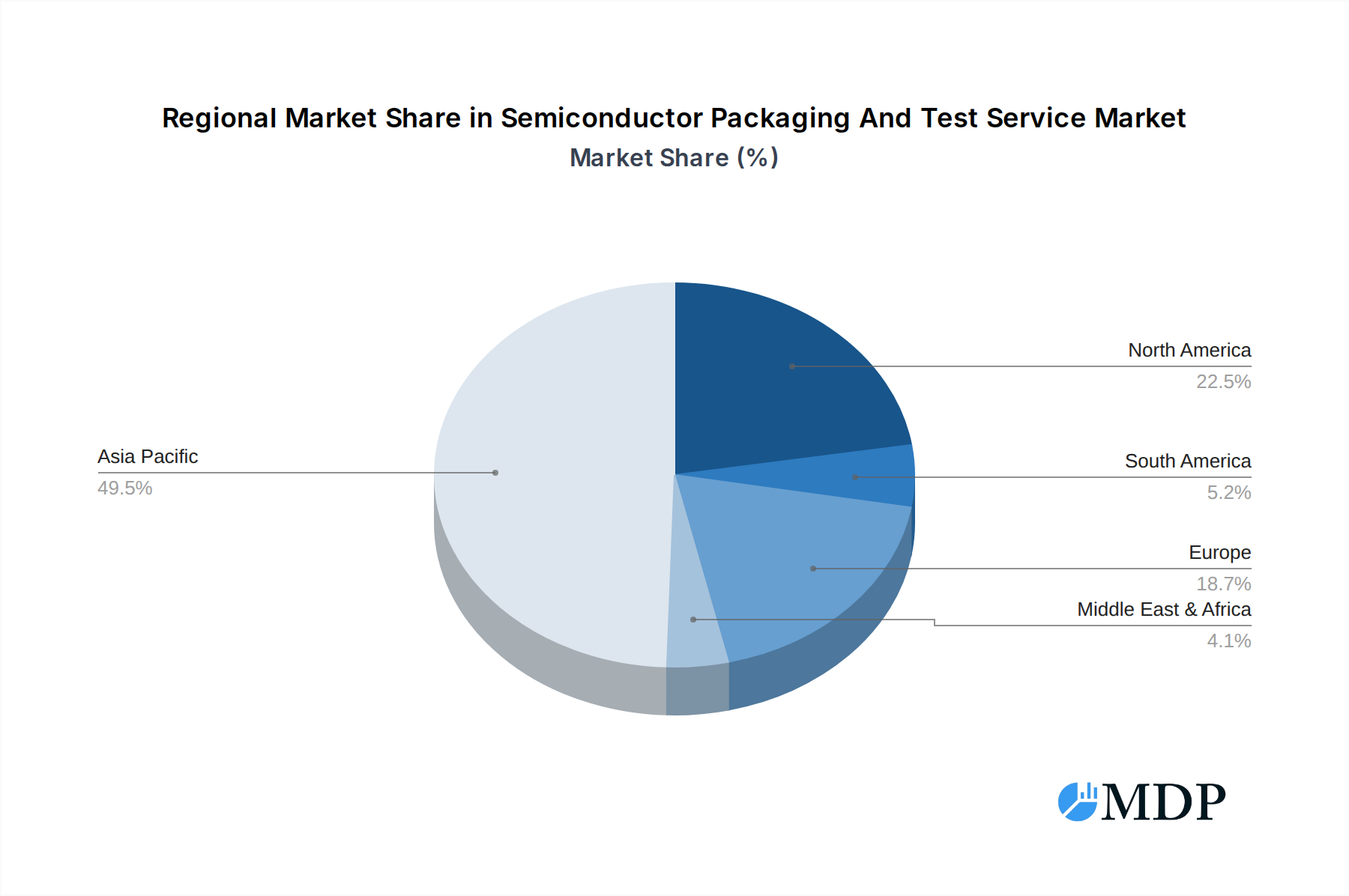
Semiconductor Packaging And Test Service Regional Market Share
Geographic Coverage of Semiconductor Packaging And Test Service
Semiconductor Packaging And Test Service REPORT HIGHLIGHTS
| Aspects | Details |
|---|---|
| Study Period | 2020-2034 |
| Base Year | 2025 |
| Estimated Year | 2026 |
| Forecast Period | 2026-2034 |
| Historical Period | 2020-2025 |
| Growth Rate | CAGR of 9.16% from 2020-2034 |
| Segmentation |
|
Table of Contents
- 1. Introduction
- 1.1. Research Scope
- 1.2. Market Segmentation
- 1.3. Research Methodology
- 1.4. Definitions and Assumptions
- 2. Executive Summary
- 2.1. Introduction
- 3. Market Dynamics
- 3.1. Introduction
- 3.2. Market Drivers
- 3.3. Market Restrains
- 3.4. Market Trends
- 4. Market Factor Analysis
- 4.1. Porters Five Forces
- 4.2. Supply/Value Chain
- 4.3. PESTEL analysis
- 4.4. Market Entropy
- 4.5. Patent/Trademark Analysis
- 5. Global Semiconductor Packaging And Test Service Analysis, Insights and Forecast, 2020-2032
- 5.1. Market Analysis, Insights and Forecast - by Application
- 5.1.1. Communication
- 5.1.2. Computing
- 5.1.3. Consumer Electronics
- 5.1.4. Others
- 5.2. Market Analysis, Insights and Forecast - by Type
- 5.2.1. Packaging Service
- 5.2.2. Test Service
- 5.3. Market Analysis, Insights and Forecast - by Region
- 5.3.1. North America
- 5.3.2. South America
- 5.3.3. Europe
- 5.3.4. Middle East & Africa
- 5.3.5. Asia Pacific
- 5.1. Market Analysis, Insights and Forecast - by Application
- 6. North America Semiconductor Packaging And Test Service Analysis, Insights and Forecast, 2020-2032
- 6.1. Market Analysis, Insights and Forecast - by Application
- 6.1.1. Communication
- 6.1.2. Computing
- 6.1.3. Consumer Electronics
- 6.1.4. Others
- 6.2. Market Analysis, Insights and Forecast - by Type
- 6.2.1. Packaging Service
- 6.2.2. Test Service
- 6.1. Market Analysis, Insights and Forecast - by Application
- 7. South America Semiconductor Packaging And Test Service Analysis, Insights and Forecast, 2020-2032
- 7.1. Market Analysis, Insights and Forecast - by Application
- 7.1.1. Communication
- 7.1.2. Computing
- 7.1.3. Consumer Electronics
- 7.1.4. Others
- 7.2. Market Analysis, Insights and Forecast - by Type
- 7.2.1. Packaging Service
- 7.2.2. Test Service
- 7.1. Market Analysis, Insights and Forecast - by Application
- 8. Europe Semiconductor Packaging And Test Service Analysis, Insights and Forecast, 2020-2032
- 8.1. Market Analysis, Insights and Forecast - by Application
- 8.1.1. Communication
- 8.1.2. Computing
- 8.1.3. Consumer Electronics
- 8.1.4. Others
- 8.2. Market Analysis, Insights and Forecast - by Type
- 8.2.1. Packaging Service
- 8.2.2. Test Service
- 8.1. Market Analysis, Insights and Forecast - by Application
- 9. Middle East & Africa Semiconductor Packaging And Test Service Analysis, Insights and Forecast, 2020-2032
- 9.1. Market Analysis, Insights and Forecast - by Application
- 9.1.1. Communication
- 9.1.2. Computing
- 9.1.3. Consumer Electronics
- 9.1.4. Others
- 9.2. Market Analysis, Insights and Forecast - by Type
- 9.2.1. Packaging Service
- 9.2.2. Test Service
- 9.1. Market Analysis, Insights and Forecast - by Application
- 10. Asia Pacific Semiconductor Packaging And Test Service Analysis, Insights and Forecast, 2020-2032
- 10.1. Market Analysis, Insights and Forecast - by Application
- 10.1.1. Communication
- 10.1.2. Computing
- 10.1.3. Consumer Electronics
- 10.1.4. Others
- 10.2. Market Analysis, Insights and Forecast - by Type
- 10.2.1. Packaging Service
- 10.2.2. Test Service
- 10.1. Market Analysis, Insights and Forecast - by Application
- 11. Competitive Analysis
- 11.1. Global Market Share Analysis 2025
- 11.2. Company Profiles
- 11.2.1 Amkor Technology
- 11.2.1.1. Overview
- 11.2.1.2. Products
- 11.2.1.3. SWOT Analysis
- 11.2.1.4. Recent Developments
- 11.2.1.5. Financials (Based on Availability)
- 11.2.2 ASE
- 11.2.2.1. Overview
- 11.2.2.2. Products
- 11.2.2.3. SWOT Analysis
- 11.2.2.4. Recent Developments
- 11.2.2.5. Financials (Based on Availability)
- 11.2.3 Powertech Technology
- 11.2.3.1. Overview
- 11.2.3.2. Products
- 11.2.3.3. SWOT Analysis
- 11.2.3.4. Recent Developments
- 11.2.3.5. Financials (Based on Availability)
- 11.2.4 Siliconware Precision Industries (SPIL)
- 11.2.4.1. Overview
- 11.2.4.2. Products
- 11.2.4.3. SWOT Analysis
- 11.2.4.4. Recent Developments
- 11.2.4.5. Financials (Based on Availability)
- 11.2.5 UTAC
- 11.2.5.1. Overview
- 11.2.5.2. Products
- 11.2.5.3. SWOT Analysis
- 11.2.5.4. Recent Developments
- 11.2.5.5. Financials (Based on Availability)
- 11.2.6 ChipMos
- 11.2.6.1. Overview
- 11.2.6.2. Products
- 11.2.6.3. SWOT Analysis
- 11.2.6.4. Recent Developments
- 11.2.6.5. Financials (Based on Availability)
- 11.2.7 Greatek
- 11.2.7.1. Overview
- 11.2.7.2. Products
- 11.2.7.3. SWOT Analysis
- 11.2.7.4. Recent Developments
- 11.2.7.5. Financials (Based on Availability)
- 11.2.8 JCET
- 11.2.8.1. Overview
- 11.2.8.2. Products
- 11.2.8.3. SWOT Analysis
- 11.2.8.4. Recent Developments
- 11.2.8.5. Financials (Based on Availability)
- 11.2.9 KYEC
- 11.2.9.1. Overview
- 11.2.9.2. Products
- 11.2.9.3. SWOT Analysis
- 11.2.9.4. Recent Developments
- 11.2.9.5. Financials (Based on Availability)
- 11.2.10 Lingsen Precision
- 11.2.10.1. Overview
- 11.2.10.2. Products
- 11.2.10.3. SWOT Analysis
- 11.2.10.4. Recent Developments
- 11.2.10.5. Financials (Based on Availability)
- 11.2.11 Tianshui Huatian (TSHT)
- 11.2.11.1. Overview
- 11.2.11.2. Products
- 11.2.11.3. SWOT Analysis
- 11.2.11.4. Recent Developments
- 11.2.11.5. Financials (Based on Availability)
- 11.2.1 Amkor Technology
List of Figures
- Figure 1: Global Semiconductor Packaging And Test Service Revenue Breakdown (undefined, %) by Region 2025 & 2033
- Figure 2: North America Semiconductor Packaging And Test Service Revenue (undefined), by Application 2025 & 2033
- Figure 3: North America Semiconductor Packaging And Test Service Revenue Share (%), by Application 2025 & 2033
- Figure 4: North America Semiconductor Packaging And Test Service Revenue (undefined), by Type 2025 & 2033
- Figure 5: North America Semiconductor Packaging And Test Service Revenue Share (%), by Type 2025 & 2033
- Figure 6: North America Semiconductor Packaging And Test Service Revenue (undefined), by Country 2025 & 2033
- Figure 7: North America Semiconductor Packaging And Test Service Revenue Share (%), by Country 2025 & 2033
- Figure 8: South America Semiconductor Packaging And Test Service Revenue (undefined), by Application 2025 & 2033
- Figure 9: South America Semiconductor Packaging And Test Service Revenue Share (%), by Application 2025 & 2033
- Figure 10: South America Semiconductor Packaging And Test Service Revenue (undefined), by Type 2025 & 2033
- Figure 11: South America Semiconductor Packaging And Test Service Revenue Share (%), by Type 2025 & 2033
- Figure 12: South America Semiconductor Packaging And Test Service Revenue (undefined), by Country 2025 & 2033
- Figure 13: South America Semiconductor Packaging And Test Service Revenue Share (%), by Country 2025 & 2033
- Figure 14: Europe Semiconductor Packaging And Test Service Revenue (undefined), by Application 2025 & 2033
- Figure 15: Europe Semiconductor Packaging And Test Service Revenue Share (%), by Application 2025 & 2033
- Figure 16: Europe Semiconductor Packaging And Test Service Revenue (undefined), by Type 2025 & 2033
- Figure 17: Europe Semiconductor Packaging And Test Service Revenue Share (%), by Type 2025 & 2033
- Figure 18: Europe Semiconductor Packaging And Test Service Revenue (undefined), by Country 2025 & 2033
- Figure 19: Europe Semiconductor Packaging And Test Service Revenue Share (%), by Country 2025 & 2033
- Figure 20: Middle East & Africa Semiconductor Packaging And Test Service Revenue (undefined), by Application 2025 & 2033
- Figure 21: Middle East & Africa Semiconductor Packaging And Test Service Revenue Share (%), by Application 2025 & 2033
- Figure 22: Middle East & Africa Semiconductor Packaging And Test Service Revenue (undefined), by Type 2025 & 2033
- Figure 23: Middle East & Africa Semiconductor Packaging And Test Service Revenue Share (%), by Type 2025 & 2033
- Figure 24: Middle East & Africa Semiconductor Packaging And Test Service Revenue (undefined), by Country 2025 & 2033
- Figure 25: Middle East & Africa Semiconductor Packaging And Test Service Revenue Share (%), by Country 2025 & 2033
- Figure 26: Asia Pacific Semiconductor Packaging And Test Service Revenue (undefined), by Application 2025 & 2033
- Figure 27: Asia Pacific Semiconductor Packaging And Test Service Revenue Share (%), by Application 2025 & 2033
- Figure 28: Asia Pacific Semiconductor Packaging And Test Service Revenue (undefined), by Type 2025 & 2033
- Figure 29: Asia Pacific Semiconductor Packaging And Test Service Revenue Share (%), by Type 2025 & 2033
- Figure 30: Asia Pacific Semiconductor Packaging And Test Service Revenue (undefined), by Country 2025 & 2033
- Figure 31: Asia Pacific Semiconductor Packaging And Test Service Revenue Share (%), by Country 2025 & 2033
List of Tables
- Table 1: Global Semiconductor Packaging And Test Service Revenue undefined Forecast, by Application 2020 & 2033
- Table 2: Global Semiconductor Packaging And Test Service Revenue undefined Forecast, by Type 2020 & 2033
- Table 3: Global Semiconductor Packaging And Test Service Revenue undefined Forecast, by Region 2020 & 2033
- Table 4: Global Semiconductor Packaging And Test Service Revenue undefined Forecast, by Application 2020 & 2033
- Table 5: Global Semiconductor Packaging And Test Service Revenue undefined Forecast, by Type 2020 & 2033
- Table 6: Global Semiconductor Packaging And Test Service Revenue undefined Forecast, by Country 2020 & 2033
- Table 7: United States Semiconductor Packaging And Test Service Revenue (undefined) Forecast, by Application 2020 & 2033
- Table 8: Canada Semiconductor Packaging And Test Service Revenue (undefined) Forecast, by Application 2020 & 2033
- Table 9: Mexico Semiconductor Packaging And Test Service Revenue (undefined) Forecast, by Application 2020 & 2033
- Table 10: Global Semiconductor Packaging And Test Service Revenue undefined Forecast, by Application 2020 & 2033
- Table 11: Global Semiconductor Packaging And Test Service Revenue undefined Forecast, by Type 2020 & 2033
- Table 12: Global Semiconductor Packaging And Test Service Revenue undefined Forecast, by Country 2020 & 2033
- Table 13: Brazil Semiconductor Packaging And Test Service Revenue (undefined) Forecast, by Application 2020 & 2033
- Table 14: Argentina Semiconductor Packaging And Test Service Revenue (undefined) Forecast, by Application 2020 & 2033
- Table 15: Rest of South America Semiconductor Packaging And Test Service Revenue (undefined) Forecast, by Application 2020 & 2033
- Table 16: Global Semiconductor Packaging And Test Service Revenue undefined Forecast, by Application 2020 & 2033
- Table 17: Global Semiconductor Packaging And Test Service Revenue undefined Forecast, by Type 2020 & 2033
- Table 18: Global Semiconductor Packaging And Test Service Revenue undefined Forecast, by Country 2020 & 2033
- Table 19: United Kingdom Semiconductor Packaging And Test Service Revenue (undefined) Forecast, by Application 2020 & 2033
- Table 20: Germany Semiconductor Packaging And Test Service Revenue (undefined) Forecast, by Application 2020 & 2033
- Table 21: France Semiconductor Packaging And Test Service Revenue (undefined) Forecast, by Application 2020 & 2033
- Table 22: Italy Semiconductor Packaging And Test Service Revenue (undefined) Forecast, by Application 2020 & 2033
- Table 23: Spain Semiconductor Packaging And Test Service Revenue (undefined) Forecast, by Application 2020 & 2033
- Table 24: Russia Semiconductor Packaging And Test Service Revenue (undefined) Forecast, by Application 2020 & 2033
- Table 25: Benelux Semiconductor Packaging And Test Service Revenue (undefined) Forecast, by Application 2020 & 2033
- Table 26: Nordics Semiconductor Packaging And Test Service Revenue (undefined) Forecast, by Application 2020 & 2033
- Table 27: Rest of Europe Semiconductor Packaging And Test Service Revenue (undefined) Forecast, by Application 2020 & 2033
- Table 28: Global Semiconductor Packaging And Test Service Revenue undefined Forecast, by Application 2020 & 2033
- Table 29: Global Semiconductor Packaging And Test Service Revenue undefined Forecast, by Type 2020 & 2033
- Table 30: Global Semiconductor Packaging And Test Service Revenue undefined Forecast, by Country 2020 & 2033
- Table 31: Turkey Semiconductor Packaging And Test Service Revenue (undefined) Forecast, by Application 2020 & 2033
- Table 32: Israel Semiconductor Packaging And Test Service Revenue (undefined) Forecast, by Application 2020 & 2033
- Table 33: GCC Semiconductor Packaging And Test Service Revenue (undefined) Forecast, by Application 2020 & 2033
- Table 34: North Africa Semiconductor Packaging And Test Service Revenue (undefined) Forecast, by Application 2020 & 2033
- Table 35: South Africa Semiconductor Packaging And Test Service Revenue (undefined) Forecast, by Application 2020 & 2033
- Table 36: Rest of Middle East & Africa Semiconductor Packaging And Test Service Revenue (undefined) Forecast, by Application 2020 & 2033
- Table 37: Global Semiconductor Packaging And Test Service Revenue undefined Forecast, by Application 2020 & 2033
- Table 38: Global Semiconductor Packaging And Test Service Revenue undefined Forecast, by Type 2020 & 2033
- Table 39: Global Semiconductor Packaging And Test Service Revenue undefined Forecast, by Country 2020 & 2033
- Table 40: China Semiconductor Packaging And Test Service Revenue (undefined) Forecast, by Application 2020 & 2033
- Table 41: India Semiconductor Packaging And Test Service Revenue (undefined) Forecast, by Application 2020 & 2033
- Table 42: Japan Semiconductor Packaging And Test Service Revenue (undefined) Forecast, by Application 2020 & 2033
- Table 43: South Korea Semiconductor Packaging And Test Service Revenue (undefined) Forecast, by Application 2020 & 2033
- Table 44: ASEAN Semiconductor Packaging And Test Service Revenue (undefined) Forecast, by Application 2020 & 2033
- Table 45: Oceania Semiconductor Packaging And Test Service Revenue (undefined) Forecast, by Application 2020 & 2033
- Table 46: Rest of Asia Pacific Semiconductor Packaging And Test Service Revenue (undefined) Forecast, by Application 2020 & 2033
Frequently Asked Questions
1. What is the projected Compound Annual Growth Rate (CAGR) of the Semiconductor Packaging And Test Service?
The projected CAGR is approximately 9.16%.
2. Which companies are prominent players in the Semiconductor Packaging And Test Service?
Key companies in the market include Amkor Technology, ASE, Powertech Technology, Siliconware Precision Industries (SPIL), UTAC, ChipMos, Greatek, JCET, KYEC, Lingsen Precision, Tianshui Huatian (TSHT).
3. What are the main segments of the Semiconductor Packaging And Test Service?
The market segments include Application, Type.
4. Can you provide details about the market size?
The market size is estimated to be USD XXX N/A as of 2022.
5. What are some drivers contributing to market growth?
N/A
6. What are the notable trends driving market growth?
N/A
7. Are there any restraints impacting market growth?
N/A
8. Can you provide examples of recent developments in the market?
N/A
9. What pricing options are available for accessing the report?
Pricing options include single-user, multi-user, and enterprise licenses priced at USD 4250.00, USD 6375.00, and USD 8500.00 respectively.
10. Is the market size provided in terms of value or volume?
The market size is provided in terms of value, measured in N/A.
11. Are there any specific market keywords associated with the report?
Yes, the market keyword associated with the report is "Semiconductor Packaging And Test Service," which aids in identifying and referencing the specific market segment covered.
12. How do I determine which pricing option suits my needs best?
The pricing options vary based on user requirements and access needs. Individual users may opt for single-user licenses, while businesses requiring broader access may choose multi-user or enterprise licenses for cost-effective access to the report.
13. Are there any additional resources or data provided in the Semiconductor Packaging And Test Service report?
While the report offers comprehensive insights, it's advisable to review the specific contents or supplementary materials provided to ascertain if additional resources or data are available.
14. How can I stay updated on further developments or reports in the Semiconductor Packaging And Test Service?
To stay informed about further developments, trends, and reports in the Semiconductor Packaging And Test Service, consider subscribing to industry newsletters, following relevant companies and organizations, or regularly checking reputable industry news sources and publications.
Methodology
Step 1 - Identification of Relevant Samples Size from Population Database


Step 2 - Approaches for Defining Global Market Size (Value, Volume* & Price*)

Note*: In applicable scenarios
Step 3 - Data Sources
Primary Research
- Web Analytics
- Survey Reports
- Research Institute
- Latest Research Reports
- Opinion Leaders
Secondary Research
- Annual Reports
- White Paper
- Latest Press Release
- Industry Association
- Paid Database
- Investor Presentations

Step 4 - Data Triangulation
Involves using different sources of information in order to increase the validity of a study
These sources are likely to be stakeholders in a program - participants, other researchers, program staff, other community members, and so on.
Then we put all data in single framework & apply various statistical tools to find out the dynamic on the market.
During the analysis stage, feedback from the stakeholder groups would be compared to determine areas of agreement as well as areas of divergence