

Key Insights
The Maskless Lithography System for Semiconductor Packaging market is poised for substantial expansion, projected to reach an estimated USD 188 million by 2025. This growth is fueled by a robust Compound Annual Growth Rate (CAGR) of 15.4% expected throughout the forecast period of 2025-2033. This dynamic trajectory is driven by an increasing demand for advanced semiconductor packaging solutions that enable miniaturization, enhanced performance, and greater functionality in electronic devices. The inherent precision and flexibility offered by maskless lithography systems are critical in meeting the evolving requirements of complex chip designs and sophisticated packaging techniques. Furthermore, the accelerating pace of technological innovation across various sectors, including consumer electronics, automotive, and telecommunications, necessitates the adoption of cutting-edge manufacturing processes like maskless lithography to keep pace with the demand for smaller, more powerful, and energy-efficient semiconductors.
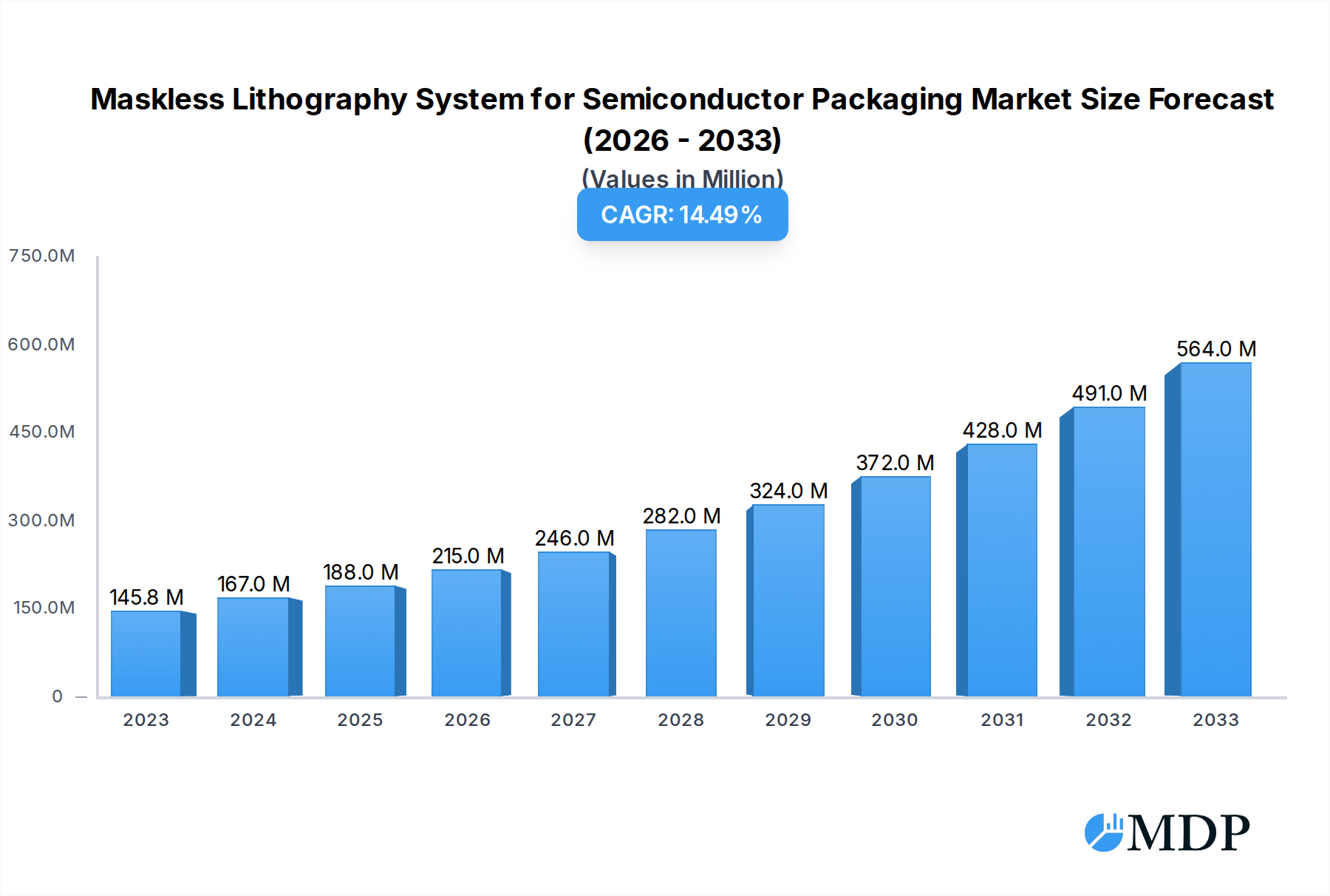
Maskless Lithography System for Semiconductor Packaging Market Size (In Million)
The market's expansion is also significantly influenced by key trends such as the growing adoption of heterogeneous integration, where different types of chips are combined into a single package, and the increasing complexity of wafer-level packaging. These advancements inherently favor maskless lithography due to its ability to directly pattern intricate designs without the need for costly and time-consuming mask fabrication. While the market shows strong upward momentum, it faces certain restraints, including the high initial investment cost associated with advanced maskless lithography equipment and the need for skilled workforce to operate and maintain these sophisticated systems. However, the long-term benefits of increased throughput, reduced lead times, and design flexibility are expected to outweigh these challenges, making maskless lithography an indispensable technology for the future of semiconductor packaging. The market is segmented into key applications like Advanced Packaging and Scientific Research, and further categorized by wafer sizes including 4&6 Inch, 8 Inch, and 12 Inch, indicating a broad spectrum of adoption across different manufacturing scales.

Maskless Lithography System for Semiconductor Packaging Company Market Share
Unlocking the Future of Semiconductor Packaging: A Comprehensive Report on Maskless Lithography Systems
This in-depth report, covering the period from 2019 to 2033 with a base and estimated year of 2025, delves into the dynamic Maskless Lithography System for Semiconductor Packaging market. We provide critical insights into market dynamics, industry trends, leading segments, product developments, growth drivers, challenges, emerging opportunities, and key players shaping this transformative technology. With projections for the forecast period 2025–2033 and historical analysis from 2019–2024, this report is an essential resource for stakeholders seeking to navigate and capitalize on the advancements in semiconductor packaging.
Maskless Lithography System for Semiconductor Packaging Market Dynamics & Concentration
The Maskless Lithography System for Semiconductor Packaging market, while still in its nascent stages of widespread adoption, exhibits a moderate concentration. Key innovation drivers include the relentless demand for miniaturization, increased functionality, and enhanced performance in electronic devices. Regulatory frameworks, particularly concerning intellectual property and environmental standards within semiconductor manufacturing, play a significant role in shaping market entry and operational strategies. Product substitutes, while not directly replacing maskless lithography for certain advanced applications, include traditional photolithography systems which continue to hold a substantial market share. End-user trends are overwhelmingly positive, driven by the burgeoning demand for 5G, AI, IoT, and high-performance computing, all of which necessitate sophisticated semiconductor packaging solutions. Mergers and acquisitions (M&A) activities are on the rise as established players seek to acquire cutting-edge technologies and expand their market reach. We anticipate at least 5 major M&A deals in the next five years, with an estimated market share shift of 15% driven by these consolidations.
Maskless Lithography System for Semiconductor Packaging Industry Trends & Analysis
The Maskless Lithography System for Semiconductor Packaging industry is poised for significant expansion, driven by a confluence of technological advancements and burgeoning market demands. The primary growth driver is the ever-increasing complexity and performance requirements of modern semiconductor devices, particularly in the realm of advanced packaging techniques like System-in-Package (SiP) and 3D integration. Maskless lithography, with its inherent flexibility and precision, offers a distinct advantage over traditional mask-based methods, enabling faster design iterations, reduced lead times, and the ability to pattern intricate designs crucial for next-generation chips. Technological disruptions are characterized by the rapid evolution of direct-write technologies, including laser-based and electron-beam lithography, offering higher resolution and throughput. Consumer preferences are indirectly influencing this market, as end-users demand more powerful, compact, and energy-efficient electronic devices, thereby pushing semiconductor manufacturers to adopt advanced packaging solutions. The competitive dynamics are intensifying, with a mix of established lithography equipment giants and innovative startups vying for market share. We project a Compound Annual Growth Rate (CAGR) of approximately 18% for the maskless lithography system market over the forecast period. Market penetration, currently estimated at 20%, is expected to surge to over 45% by 2033. The elimination of mask-related costs and lead times is a significant advantage, allowing for more agile product development cycles, which is a key factor in gaining market share.
Leading Markets & Segments in Maskless Lithography System for Semiconductor Packaging
The Advanced Packaging segment within the Maskless Lithography System for Semiconductor Packaging market is currently the dominant force, driven by the insatiable demand for higher performance and greater integration capabilities in electronic devices. This segment encompasses applications critical for 5G infrastructure, artificial intelligence accelerators, high-performance computing, and advanced consumer electronics. The 4&6 Inch wafer size segment is witnessing substantial growth due to its suitability for niche, high-value applications and its alignment with the production of specialized sensors and MEMS devices. The economic policies supporting domestic semiconductor manufacturing, coupled with significant infrastructure investments in regions like Asia-Pacific, are major catalysts.
Advanced Packaging Dominance:
- Key Drivers: Increasing complexity of chip designs, need for heterogeneous integration, demand for smaller and more powerful electronic devices.
- Detailed Analysis: The transition from traditional 2D chip architectures to advanced 2.5D and 3D packaging technologies necessitates lithography solutions that can handle finer features and complex interconnects, a forte of maskless systems. This allows for the integration of multiple chiplets onto a single package, significantly boosting performance and reducing form factor. The growth of data centers, AI training, and edge computing further fuels the demand for advanced packaging solutions.
4&6 Inch Wafer Size Segment Growth:
- Key Drivers: Production of specialized sensors, MEMS devices, and optoelectronics where cost-effectiveness and flexibility are paramount.
- Detailed Analysis: While larger wafer sizes dominate mainstream semiconductor production, the 4&6 inch segments are crucial for specific, high-margin applications. Maskless lithography provides the flexibility to pattern intricate designs on these smaller wafers without the prohibitive cost of mask development, making it an ideal solution for R&D and pilot production of novel devices.
Emerging Trends in 8 Inch and 12 Inch Segments:
- Key Drivers: Growing adoption of maskless lithography for certain advanced processes on larger wafers, cost reduction initiatives in established foundries.
- Detailed Analysis: As maskless lithography technologies mature and their throughput increases, there is a growing interest in their application for specific process steps on 8-inch and even 12-inch wafers, particularly for applications requiring high flexibility and rapid prototyping, thereby pushing for wider adoption across the semiconductor manufacturing spectrum.
Maskless Lithography System for Semiconductor Packaging Product Developments
Product developments in maskless lithography systems are characterized by enhanced resolution, increased throughput, and greater flexibility. Innovations are focused on direct-write technologies, including advanced laser direct imaging (LDI) and multi-beam electron-beam lithography, offering sub-micron patterning capabilities. These advancements enable manufacturers to achieve finer feature sizes essential for advanced packaging and R&D. The competitive advantage lies in the ability to rapidly iterate designs, reduce mask-related costs and lead times, and support complex, multi-layer interconnects crucial for next-generation semiconductor devices.
Key Drivers of Maskless Lithography System for Semiconductor Packaging Growth
The growth of the Maskless Lithography System for Semiconductor Packaging market is propelled by several key factors. Technological advancements in direct-write lithography, offering higher precision and speed, are paramount. The escalating demand for sophisticated semiconductor packaging solutions to enable higher performance, miniaturization, and energy efficiency in electronic devices, driven by 5G, AI, and IoT, is a significant catalyst. Furthermore, government initiatives and investments aimed at bolstering domestic semiconductor manufacturing capabilities and supply chain resilience are providing a supportive ecosystem for the adoption of advanced lithography technologies.
Challenges in the Maskless Lithography System for Semiconductor Packaging Market
Despite the promising growth trajectory, the Maskless Lithography System for Semiconductor Packaging market faces several challenges. High initial capital investment for advanced systems remains a barrier for smaller manufacturers. The technical complexity and need for specialized expertise in operating and maintaining these systems can also be a constraint. While improving, the throughput of some maskless technologies may still not match traditional mask-based lithography for high-volume, standardized production runs, creating a performance dilemma. Furthermore, ensuring interoperability with existing fabrication workflows and stringent quality control for high-yield manufacturing are ongoing challenges.
Emerging Opportunities in Maskless Lithography System for Semiconductor Packaging
Emerging opportunities in the Maskless Lithography System for Semiconductor Packaging market are abundant, fueled by continuous technological breakthroughs and strategic market expansion. The development of novel materials and process integration techniques is opening new avenues for finer patterning and enhanced device performance. Strategic partnerships between lithography equipment manufacturers, semiconductor foundries, and R&D institutions are crucial for co-developing customized solutions and accelerating technology adoption. Market expansion into emerging applications such as advanced display technologies and biomedical devices presents significant long-term growth potential.
Leading Players in the Maskless Lithography System for Semiconductor Packaging Sector
- SCREEN
- USHIO
- Heidelberg Instruments
- ORC Manufacturing
- Visitech
- EV Group (EVG)
- Circuit Fabology Microelectronics Equipment
- Jiangsu Ysphotech Integrated Circuit Equipment
Key Milestones in Maskless Lithography System for Semiconductor Packaging Industry
- 2019: Significant advancements in laser direct imaging (LDI) technology reported, offering improved resolution for advanced packaging applications.
- 2020: Introduction of multi-beam electron-beam lithography systems with enhanced throughput capabilities.
- 2021: Increased investment in R&D by major players to develop next-generation maskless lithography solutions for 3D integration.
- 2022: Strategic partnerships formed between equipment manufacturers and leading semiconductor foundries to accelerate technology validation.
- 2023: First commercial deployments of advanced maskless lithography systems for high-volume advanced packaging production.
- 2024: Growing interest in the application of maskless lithography for novel materials and processes in scientific research.
Strategic Outlook for Maskless Lithography System for Semiconductor Packaging Market
The strategic outlook for the Maskless Lithography System for Semiconductor Packaging market is exceptionally positive, driven by ongoing innovation and the increasing necessity for advanced semiconductor packaging. Future market growth will be accelerated by the continuous refinement of direct-write technologies, enabling finer feature sizes and higher throughput. Strategic opportunities lie in expanding the application of maskless lithography beyond traditional semiconductor packaging into emerging fields such as flexible electronics, advanced displays, and microfluidics. Collaborations to develop standardized protocols and interoperable solutions will be crucial for widespread adoption and sustained market expansion.
Maskless Lithography System for Semiconductor Packaging Segmentation
-
1. Application
- 1.1. Advanced Packaging
- 1.2. Scientific Research
-
2. Types
- 2.1. 4&6 Inch
- 2.2. 8 Inch
- 2.3. 12 Inch
Maskless Lithography System for Semiconductor Packaging Segmentation By Geography
-
1. North America
- 1.1. United States
- 1.2. Canada
- 1.3. Mexico
-
2. South America
- 2.1. Brazil
- 2.2. Argentina
- 2.3. Rest of South America
-
3. Europe
- 3.1. United Kingdom
- 3.2. Germany
- 3.3. France
- 3.4. Italy
- 3.5. Spain
- 3.6. Russia
- 3.7. Benelux
- 3.8. Nordics
- 3.9. Rest of Europe
-
4. Middle East & Africa
- 4.1. Turkey
- 4.2. Israel
- 4.3. GCC
- 4.4. North Africa
- 4.5. South Africa
- 4.6. Rest of Middle East & Africa
-
5. Asia Pacific
- 5.1. China
- 5.2. India
- 5.3. Japan
- 5.4. South Korea
- 5.5. ASEAN
- 5.6. Oceania
- 5.7. Rest of Asia Pacific
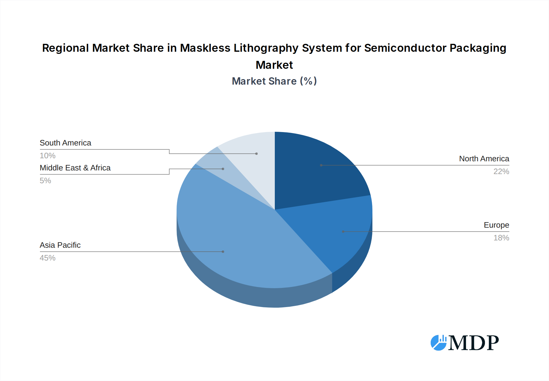
Maskless Lithography System for Semiconductor Packaging Regional Market Share
Geographic Coverage of Maskless Lithography System for Semiconductor Packaging
Maskless Lithography System for Semiconductor Packaging REPORT HIGHLIGHTS
| Aspects | Details |
|---|---|
| Study Period | 2020-2034 |
| Base Year | 2025 |
| Estimated Year | 2026 |
| Forecast Period | 2026-2034 |
| Historical Period | 2020-2025 |
| Growth Rate | CAGR of 15.4% from 2020-2034 |
| Segmentation |
|
Table of Contents
- 1. Introduction
- 1.1. Research Scope
- 1.2. Market Segmentation
- 1.3. Research Methodology
- 1.4. Definitions and Assumptions
- 2. Executive Summary
- 2.1. Introduction
- 3. Market Dynamics
- 3.1. Introduction
- 3.2. Market Drivers
- 3.3. Market Restrains
- 3.4. Market Trends
- 4. Market Factor Analysis
- 4.1. Porters Five Forces
- 4.2. Supply/Value Chain
- 4.3. PESTEL analysis
- 4.4. Market Entropy
- 4.5. Patent/Trademark Analysis
- 5. Global Maskless Lithography System for Semiconductor Packaging Analysis, Insights and Forecast, 2020-2032
- 5.1. Market Analysis, Insights and Forecast - by Application
- 5.1.1. Advanced Packaging
- 5.1.2. Scientific Research
- 5.2. Market Analysis, Insights and Forecast - by Types
- 5.2.1. 4&6 Inch
- 5.2.2. 8 Inch
- 5.2.3. 12 Inch
- 5.3. Market Analysis, Insights and Forecast - by Region
- 5.3.1. North America
- 5.3.2. South America
- 5.3.3. Europe
- 5.3.4. Middle East & Africa
- 5.3.5. Asia Pacific
- 5.1. Market Analysis, Insights and Forecast - by Application
- 6. North America Maskless Lithography System for Semiconductor Packaging Analysis, Insights and Forecast, 2020-2032
- 6.1. Market Analysis, Insights and Forecast - by Application
- 6.1.1. Advanced Packaging
- 6.1.2. Scientific Research
- 6.2. Market Analysis, Insights and Forecast - by Types
- 6.2.1. 4&6 Inch
- 6.2.2. 8 Inch
- 6.2.3. 12 Inch
- 6.1. Market Analysis, Insights and Forecast - by Application
- 7. South America Maskless Lithography System for Semiconductor Packaging Analysis, Insights and Forecast, 2020-2032
- 7.1. Market Analysis, Insights and Forecast - by Application
- 7.1.1. Advanced Packaging
- 7.1.2. Scientific Research
- 7.2. Market Analysis, Insights and Forecast - by Types
- 7.2.1. 4&6 Inch
- 7.2.2. 8 Inch
- 7.2.3. 12 Inch
- 7.1. Market Analysis, Insights and Forecast - by Application
- 8. Europe Maskless Lithography System for Semiconductor Packaging Analysis, Insights and Forecast, 2020-2032
- 8.1. Market Analysis, Insights and Forecast - by Application
- 8.1.1. Advanced Packaging
- 8.1.2. Scientific Research
- 8.2. Market Analysis, Insights and Forecast - by Types
- 8.2.1. 4&6 Inch
- 8.2.2. 8 Inch
- 8.2.3. 12 Inch
- 8.1. Market Analysis, Insights and Forecast - by Application
- 9. Middle East & Africa Maskless Lithography System for Semiconductor Packaging Analysis, Insights and Forecast, 2020-2032
- 9.1. Market Analysis, Insights and Forecast - by Application
- 9.1.1. Advanced Packaging
- 9.1.2. Scientific Research
- 9.2. Market Analysis, Insights and Forecast - by Types
- 9.2.1. 4&6 Inch
- 9.2.2. 8 Inch
- 9.2.3. 12 Inch
- 9.1. Market Analysis, Insights and Forecast - by Application
- 10. Asia Pacific Maskless Lithography System for Semiconductor Packaging Analysis, Insights and Forecast, 2020-2032
- 10.1. Market Analysis, Insights and Forecast - by Application
- 10.1.1. Advanced Packaging
- 10.1.2. Scientific Research
- 10.2. Market Analysis, Insights and Forecast - by Types
- 10.2.1. 4&6 Inch
- 10.2.2. 8 Inch
- 10.2.3. 12 Inch
- 10.1. Market Analysis, Insights and Forecast - by Application
- 11. Competitive Analysis
- 11.1. Global Market Share Analysis 2025
- 11.2. Company Profiles
- 11.2.1 SCREEN
- 11.2.1.1. Overview
- 11.2.1.2. Products
- 11.2.1.3. SWOT Analysis
- 11.2.1.4. Recent Developments
- 11.2.1.5. Financials (Based on Availability)
- 11.2.2 USHIO
- 11.2.2.1. Overview
- 11.2.2.2. Products
- 11.2.2.3. SWOT Analysis
- 11.2.2.4. Recent Developments
- 11.2.2.5. Financials (Based on Availability)
- 11.2.3 Heidelberg Instruments
- 11.2.3.1. Overview
- 11.2.3.2. Products
- 11.2.3.3. SWOT Analysis
- 11.2.3.4. Recent Developments
- 11.2.3.5. Financials (Based on Availability)
- 11.2.4 ORC Manufacturing
- 11.2.4.1. Overview
- 11.2.4.2. Products
- 11.2.4.3. SWOT Analysis
- 11.2.4.4. Recent Developments
- 11.2.4.5. Financials (Based on Availability)
- 11.2.5 Visitech
- 11.2.5.1. Overview
- 11.2.5.2. Products
- 11.2.5.3. SWOT Analysis
- 11.2.5.4. Recent Developments
- 11.2.5.5. Financials (Based on Availability)
- 11.2.6 EV Group (EVG)
- 11.2.6.1. Overview
- 11.2.6.2. Products
- 11.2.6.3. SWOT Analysis
- 11.2.6.4. Recent Developments
- 11.2.6.5. Financials (Based on Availability)
- 11.2.7 Circuit Fabology Microelectronics Equipment
- 11.2.7.1. Overview
- 11.2.7.2. Products
- 11.2.7.3. SWOT Analysis
- 11.2.7.4. Recent Developments
- 11.2.7.5. Financials (Based on Availability)
- 11.2.8 Jiangsu Ysphotech Integrated Circuit Equipment
- 11.2.8.1. Overview
- 11.2.8.2. Products
- 11.2.8.3. SWOT Analysis
- 11.2.8.4. Recent Developments
- 11.2.8.5. Financials (Based on Availability)
- 11.2.1 SCREEN
List of Figures
- Figure 1: Global Maskless Lithography System for Semiconductor Packaging Revenue Breakdown (million, %) by Region 2025 & 2033
- Figure 2: Global Maskless Lithography System for Semiconductor Packaging Volume Breakdown (K, %) by Region 2025 & 2033
- Figure 3: North America Maskless Lithography System for Semiconductor Packaging Revenue (million), by Application 2025 & 2033
- Figure 4: North America Maskless Lithography System for Semiconductor Packaging Volume (K), by Application 2025 & 2033
- Figure 5: North America Maskless Lithography System for Semiconductor Packaging Revenue Share (%), by Application 2025 & 2033
- Figure 6: North America Maskless Lithography System for Semiconductor Packaging Volume Share (%), by Application 2025 & 2033
- Figure 7: North America Maskless Lithography System for Semiconductor Packaging Revenue (million), by Types 2025 & 2033
- Figure 8: North America Maskless Lithography System for Semiconductor Packaging Volume (K), by Types 2025 & 2033
- Figure 9: North America Maskless Lithography System for Semiconductor Packaging Revenue Share (%), by Types 2025 & 2033
- Figure 10: North America Maskless Lithography System for Semiconductor Packaging Volume Share (%), by Types 2025 & 2033
- Figure 11: North America Maskless Lithography System for Semiconductor Packaging Revenue (million), by Country 2025 & 2033
- Figure 12: North America Maskless Lithography System for Semiconductor Packaging Volume (K), by Country 2025 & 2033
- Figure 13: North America Maskless Lithography System for Semiconductor Packaging Revenue Share (%), by Country 2025 & 2033
- Figure 14: North America Maskless Lithography System for Semiconductor Packaging Volume Share (%), by Country 2025 & 2033
- Figure 15: South America Maskless Lithography System for Semiconductor Packaging Revenue (million), by Application 2025 & 2033
- Figure 16: South America Maskless Lithography System for Semiconductor Packaging Volume (K), by Application 2025 & 2033
- Figure 17: South America Maskless Lithography System for Semiconductor Packaging Revenue Share (%), by Application 2025 & 2033
- Figure 18: South America Maskless Lithography System for Semiconductor Packaging Volume Share (%), by Application 2025 & 2033
- Figure 19: South America Maskless Lithography System for Semiconductor Packaging Revenue (million), by Types 2025 & 2033
- Figure 20: South America Maskless Lithography System for Semiconductor Packaging Volume (K), by Types 2025 & 2033
- Figure 21: South America Maskless Lithography System for Semiconductor Packaging Revenue Share (%), by Types 2025 & 2033
- Figure 22: South America Maskless Lithography System for Semiconductor Packaging Volume Share (%), by Types 2025 & 2033
- Figure 23: South America Maskless Lithography System for Semiconductor Packaging Revenue (million), by Country 2025 & 2033
- Figure 24: South America Maskless Lithography System for Semiconductor Packaging Volume (K), by Country 2025 & 2033
- Figure 25: South America Maskless Lithography System for Semiconductor Packaging Revenue Share (%), by Country 2025 & 2033
- Figure 26: South America Maskless Lithography System for Semiconductor Packaging Volume Share (%), by Country 2025 & 2033
- Figure 27: Europe Maskless Lithography System for Semiconductor Packaging Revenue (million), by Application 2025 & 2033
- Figure 28: Europe Maskless Lithography System for Semiconductor Packaging Volume (K), by Application 2025 & 2033
- Figure 29: Europe Maskless Lithography System for Semiconductor Packaging Revenue Share (%), by Application 2025 & 2033
- Figure 30: Europe Maskless Lithography System for Semiconductor Packaging Volume Share (%), by Application 2025 & 2033
- Figure 31: Europe Maskless Lithography System for Semiconductor Packaging Revenue (million), by Types 2025 & 2033
- Figure 32: Europe Maskless Lithography System for Semiconductor Packaging Volume (K), by Types 2025 & 2033
- Figure 33: Europe Maskless Lithography System for Semiconductor Packaging Revenue Share (%), by Types 2025 & 2033
- Figure 34: Europe Maskless Lithography System for Semiconductor Packaging Volume Share (%), by Types 2025 & 2033
- Figure 35: Europe Maskless Lithography System for Semiconductor Packaging Revenue (million), by Country 2025 & 2033
- Figure 36: Europe Maskless Lithography System for Semiconductor Packaging Volume (K), by Country 2025 & 2033
- Figure 37: Europe Maskless Lithography System for Semiconductor Packaging Revenue Share (%), by Country 2025 & 2033
- Figure 38: Europe Maskless Lithography System for Semiconductor Packaging Volume Share (%), by Country 2025 & 2033
- Figure 39: Middle East & Africa Maskless Lithography System for Semiconductor Packaging Revenue (million), by Application 2025 & 2033
- Figure 40: Middle East & Africa Maskless Lithography System for Semiconductor Packaging Volume (K), by Application 2025 & 2033
- Figure 41: Middle East & Africa Maskless Lithography System for Semiconductor Packaging Revenue Share (%), by Application 2025 & 2033
- Figure 42: Middle East & Africa Maskless Lithography System for Semiconductor Packaging Volume Share (%), by Application 2025 & 2033
- Figure 43: Middle East & Africa Maskless Lithography System for Semiconductor Packaging Revenue (million), by Types 2025 & 2033
- Figure 44: Middle East & Africa Maskless Lithography System for Semiconductor Packaging Volume (K), by Types 2025 & 2033
- Figure 45: Middle East & Africa Maskless Lithography System for Semiconductor Packaging Revenue Share (%), by Types 2025 & 2033
- Figure 46: Middle East & Africa Maskless Lithography System for Semiconductor Packaging Volume Share (%), by Types 2025 & 2033
- Figure 47: Middle East & Africa Maskless Lithography System for Semiconductor Packaging Revenue (million), by Country 2025 & 2033
- Figure 48: Middle East & Africa Maskless Lithography System for Semiconductor Packaging Volume (K), by Country 2025 & 2033
- Figure 49: Middle East & Africa Maskless Lithography System for Semiconductor Packaging Revenue Share (%), by Country 2025 & 2033
- Figure 50: Middle East & Africa Maskless Lithography System for Semiconductor Packaging Volume Share (%), by Country 2025 & 2033
- Figure 51: Asia Pacific Maskless Lithography System for Semiconductor Packaging Revenue (million), by Application 2025 & 2033
- Figure 52: Asia Pacific Maskless Lithography System for Semiconductor Packaging Volume (K), by Application 2025 & 2033
- Figure 53: Asia Pacific Maskless Lithography System for Semiconductor Packaging Revenue Share (%), by Application 2025 & 2033
- Figure 54: Asia Pacific Maskless Lithography System for Semiconductor Packaging Volume Share (%), by Application 2025 & 2033
- Figure 55: Asia Pacific Maskless Lithography System for Semiconductor Packaging Revenue (million), by Types 2025 & 2033
- Figure 56: Asia Pacific Maskless Lithography System for Semiconductor Packaging Volume (K), by Types 2025 & 2033
- Figure 57: Asia Pacific Maskless Lithography System for Semiconductor Packaging Revenue Share (%), by Types 2025 & 2033
- Figure 58: Asia Pacific Maskless Lithography System for Semiconductor Packaging Volume Share (%), by Types 2025 & 2033
- Figure 59: Asia Pacific Maskless Lithography System for Semiconductor Packaging Revenue (million), by Country 2025 & 2033
- Figure 60: Asia Pacific Maskless Lithography System for Semiconductor Packaging Volume (K), by Country 2025 & 2033
- Figure 61: Asia Pacific Maskless Lithography System for Semiconductor Packaging Revenue Share (%), by Country 2025 & 2033
- Figure 62: Asia Pacific Maskless Lithography System for Semiconductor Packaging Volume Share (%), by Country 2025 & 2033
List of Tables
- Table 1: Global Maskless Lithography System for Semiconductor Packaging Revenue million Forecast, by Application 2020 & 2033
- Table 2: Global Maskless Lithography System for Semiconductor Packaging Volume K Forecast, by Application 2020 & 2033
- Table 3: Global Maskless Lithography System for Semiconductor Packaging Revenue million Forecast, by Types 2020 & 2033
- Table 4: Global Maskless Lithography System for Semiconductor Packaging Volume K Forecast, by Types 2020 & 2033
- Table 5: Global Maskless Lithography System for Semiconductor Packaging Revenue million Forecast, by Region 2020 & 2033
- Table 6: Global Maskless Lithography System for Semiconductor Packaging Volume K Forecast, by Region 2020 & 2033
- Table 7: Global Maskless Lithography System for Semiconductor Packaging Revenue million Forecast, by Application 2020 & 2033
- Table 8: Global Maskless Lithography System for Semiconductor Packaging Volume K Forecast, by Application 2020 & 2033
- Table 9: Global Maskless Lithography System for Semiconductor Packaging Revenue million Forecast, by Types 2020 & 2033
- Table 10: Global Maskless Lithography System for Semiconductor Packaging Volume K Forecast, by Types 2020 & 2033
- Table 11: Global Maskless Lithography System for Semiconductor Packaging Revenue million Forecast, by Country 2020 & 2033
- Table 12: Global Maskless Lithography System for Semiconductor Packaging Volume K Forecast, by Country 2020 & 2033
- Table 13: United States Maskless Lithography System for Semiconductor Packaging Revenue (million) Forecast, by Application 2020 & 2033
- Table 14: United States Maskless Lithography System for Semiconductor Packaging Volume (K) Forecast, by Application 2020 & 2033
- Table 15: Canada Maskless Lithography System for Semiconductor Packaging Revenue (million) Forecast, by Application 2020 & 2033
- Table 16: Canada Maskless Lithography System for Semiconductor Packaging Volume (K) Forecast, by Application 2020 & 2033
- Table 17: Mexico Maskless Lithography System for Semiconductor Packaging Revenue (million) Forecast, by Application 2020 & 2033
- Table 18: Mexico Maskless Lithography System for Semiconductor Packaging Volume (K) Forecast, by Application 2020 & 2033
- Table 19: Global Maskless Lithography System for Semiconductor Packaging Revenue million Forecast, by Application 2020 & 2033
- Table 20: Global Maskless Lithography System for Semiconductor Packaging Volume K Forecast, by Application 2020 & 2033
- Table 21: Global Maskless Lithography System for Semiconductor Packaging Revenue million Forecast, by Types 2020 & 2033
- Table 22: Global Maskless Lithography System for Semiconductor Packaging Volume K Forecast, by Types 2020 & 2033
- Table 23: Global Maskless Lithography System for Semiconductor Packaging Revenue million Forecast, by Country 2020 & 2033
- Table 24: Global Maskless Lithography System for Semiconductor Packaging Volume K Forecast, by Country 2020 & 2033
- Table 25: Brazil Maskless Lithography System for Semiconductor Packaging Revenue (million) Forecast, by Application 2020 & 2033
- Table 26: Brazil Maskless Lithography System for Semiconductor Packaging Volume (K) Forecast, by Application 2020 & 2033
- Table 27: Argentina Maskless Lithography System for Semiconductor Packaging Revenue (million) Forecast, by Application 2020 & 2033
- Table 28: Argentina Maskless Lithography System for Semiconductor Packaging Volume (K) Forecast, by Application 2020 & 2033
- Table 29: Rest of South America Maskless Lithography System for Semiconductor Packaging Revenue (million) Forecast, by Application 2020 & 2033
- Table 30: Rest of South America Maskless Lithography System for Semiconductor Packaging Volume (K) Forecast, by Application 2020 & 2033
- Table 31: Global Maskless Lithography System for Semiconductor Packaging Revenue million Forecast, by Application 2020 & 2033
- Table 32: Global Maskless Lithography System for Semiconductor Packaging Volume K Forecast, by Application 2020 & 2033
- Table 33: Global Maskless Lithography System for Semiconductor Packaging Revenue million Forecast, by Types 2020 & 2033
- Table 34: Global Maskless Lithography System for Semiconductor Packaging Volume K Forecast, by Types 2020 & 2033
- Table 35: Global Maskless Lithography System for Semiconductor Packaging Revenue million Forecast, by Country 2020 & 2033
- Table 36: Global Maskless Lithography System for Semiconductor Packaging Volume K Forecast, by Country 2020 & 2033
- Table 37: United Kingdom Maskless Lithography System for Semiconductor Packaging Revenue (million) Forecast, by Application 2020 & 2033
- Table 38: United Kingdom Maskless Lithography System for Semiconductor Packaging Volume (K) Forecast, by Application 2020 & 2033
- Table 39: Germany Maskless Lithography System for Semiconductor Packaging Revenue (million) Forecast, by Application 2020 & 2033
- Table 40: Germany Maskless Lithography System for Semiconductor Packaging Volume (K) Forecast, by Application 2020 & 2033
- Table 41: France Maskless Lithography System for Semiconductor Packaging Revenue (million) Forecast, by Application 2020 & 2033
- Table 42: France Maskless Lithography System for Semiconductor Packaging Volume (K) Forecast, by Application 2020 & 2033
- Table 43: Italy Maskless Lithography System for Semiconductor Packaging Revenue (million) Forecast, by Application 2020 & 2033
- Table 44: Italy Maskless Lithography System for Semiconductor Packaging Volume (K) Forecast, by Application 2020 & 2033
- Table 45: Spain Maskless Lithography System for Semiconductor Packaging Revenue (million) Forecast, by Application 2020 & 2033
- Table 46: Spain Maskless Lithography System for Semiconductor Packaging Volume (K) Forecast, by Application 2020 & 2033
- Table 47: Russia Maskless Lithography System for Semiconductor Packaging Revenue (million) Forecast, by Application 2020 & 2033
- Table 48: Russia Maskless Lithography System for Semiconductor Packaging Volume (K) Forecast, by Application 2020 & 2033
- Table 49: Benelux Maskless Lithography System for Semiconductor Packaging Revenue (million) Forecast, by Application 2020 & 2033
- Table 50: Benelux Maskless Lithography System for Semiconductor Packaging Volume (K) Forecast, by Application 2020 & 2033
- Table 51: Nordics Maskless Lithography System for Semiconductor Packaging Revenue (million) Forecast, by Application 2020 & 2033
- Table 52: Nordics Maskless Lithography System for Semiconductor Packaging Volume (K) Forecast, by Application 2020 & 2033
- Table 53: Rest of Europe Maskless Lithography System for Semiconductor Packaging Revenue (million) Forecast, by Application 2020 & 2033
- Table 54: Rest of Europe Maskless Lithography System for Semiconductor Packaging Volume (K) Forecast, by Application 2020 & 2033
- Table 55: Global Maskless Lithography System for Semiconductor Packaging Revenue million Forecast, by Application 2020 & 2033
- Table 56: Global Maskless Lithography System for Semiconductor Packaging Volume K Forecast, by Application 2020 & 2033
- Table 57: Global Maskless Lithography System for Semiconductor Packaging Revenue million Forecast, by Types 2020 & 2033
- Table 58: Global Maskless Lithography System for Semiconductor Packaging Volume K Forecast, by Types 2020 & 2033
- Table 59: Global Maskless Lithography System for Semiconductor Packaging Revenue million Forecast, by Country 2020 & 2033
- Table 60: Global Maskless Lithography System for Semiconductor Packaging Volume K Forecast, by Country 2020 & 2033
- Table 61: Turkey Maskless Lithography System for Semiconductor Packaging Revenue (million) Forecast, by Application 2020 & 2033
- Table 62: Turkey Maskless Lithography System for Semiconductor Packaging Volume (K) Forecast, by Application 2020 & 2033
- Table 63: Israel Maskless Lithography System for Semiconductor Packaging Revenue (million) Forecast, by Application 2020 & 2033
- Table 64: Israel Maskless Lithography System for Semiconductor Packaging Volume (K) Forecast, by Application 2020 & 2033
- Table 65: GCC Maskless Lithography System for Semiconductor Packaging Revenue (million) Forecast, by Application 2020 & 2033
- Table 66: GCC Maskless Lithography System for Semiconductor Packaging Volume (K) Forecast, by Application 2020 & 2033
- Table 67: North Africa Maskless Lithography System for Semiconductor Packaging Revenue (million) Forecast, by Application 2020 & 2033
- Table 68: North Africa Maskless Lithography System for Semiconductor Packaging Volume (K) Forecast, by Application 2020 & 2033
- Table 69: South Africa Maskless Lithography System for Semiconductor Packaging Revenue (million) Forecast, by Application 2020 & 2033
- Table 70: South Africa Maskless Lithography System for Semiconductor Packaging Volume (K) Forecast, by Application 2020 & 2033
- Table 71: Rest of Middle East & Africa Maskless Lithography System for Semiconductor Packaging Revenue (million) Forecast, by Application 2020 & 2033
- Table 72: Rest of Middle East & Africa Maskless Lithography System for Semiconductor Packaging Volume (K) Forecast, by Application 2020 & 2033
- Table 73: Global Maskless Lithography System for Semiconductor Packaging Revenue million Forecast, by Application 2020 & 2033
- Table 74: Global Maskless Lithography System for Semiconductor Packaging Volume K Forecast, by Application 2020 & 2033
- Table 75: Global Maskless Lithography System for Semiconductor Packaging Revenue million Forecast, by Types 2020 & 2033
- Table 76: Global Maskless Lithography System for Semiconductor Packaging Volume K Forecast, by Types 2020 & 2033
- Table 77: Global Maskless Lithography System for Semiconductor Packaging Revenue million Forecast, by Country 2020 & 2033
- Table 78: Global Maskless Lithography System for Semiconductor Packaging Volume K Forecast, by Country 2020 & 2033
- Table 79: China Maskless Lithography System for Semiconductor Packaging Revenue (million) Forecast, by Application 2020 & 2033
- Table 80: China Maskless Lithography System for Semiconductor Packaging Volume (K) Forecast, by Application 2020 & 2033
- Table 81: India Maskless Lithography System for Semiconductor Packaging Revenue (million) Forecast, by Application 2020 & 2033
- Table 82: India Maskless Lithography System for Semiconductor Packaging Volume (K) Forecast, by Application 2020 & 2033
- Table 83: Japan Maskless Lithography System for Semiconductor Packaging Revenue (million) Forecast, by Application 2020 & 2033
- Table 84: Japan Maskless Lithography System for Semiconductor Packaging Volume (K) Forecast, by Application 2020 & 2033
- Table 85: South Korea Maskless Lithography System for Semiconductor Packaging Revenue (million) Forecast, by Application 2020 & 2033
- Table 86: South Korea Maskless Lithography System for Semiconductor Packaging Volume (K) Forecast, by Application 2020 & 2033
- Table 87: ASEAN Maskless Lithography System for Semiconductor Packaging Revenue (million) Forecast, by Application 2020 & 2033
- Table 88: ASEAN Maskless Lithography System for Semiconductor Packaging Volume (K) Forecast, by Application 2020 & 2033
- Table 89: Oceania Maskless Lithography System for Semiconductor Packaging Revenue (million) Forecast, by Application 2020 & 2033
- Table 90: Oceania Maskless Lithography System for Semiconductor Packaging Volume (K) Forecast, by Application 2020 & 2033
- Table 91: Rest of Asia Pacific Maskless Lithography System for Semiconductor Packaging Revenue (million) Forecast, by Application 2020 & 2033
- Table 92: Rest of Asia Pacific Maskless Lithography System for Semiconductor Packaging Volume (K) Forecast, by Application 2020 & 2033
Frequently Asked Questions
1. What is the projected Compound Annual Growth Rate (CAGR) of the Maskless Lithography System for Semiconductor Packaging?
The projected CAGR is approximately 15.4%.
2. Which companies are prominent players in the Maskless Lithography System for Semiconductor Packaging?
Key companies in the market include SCREEN, USHIO, Heidelberg Instruments, ORC Manufacturing, Visitech, EV Group (EVG), Circuit Fabology Microelectronics Equipment, Jiangsu Ysphotech Integrated Circuit Equipment.
3. What are the main segments of the Maskless Lithography System for Semiconductor Packaging?
The market segments include Application, Types.
4. Can you provide details about the market size?
The market size is estimated to be USD 188 million as of 2022.
5. What are some drivers contributing to market growth?
N/A
6. What are the notable trends driving market growth?
N/A
7. Are there any restraints impacting market growth?
N/A
8. Can you provide examples of recent developments in the market?
N/A
9. What pricing options are available for accessing the report?
Pricing options include single-user, multi-user, and enterprise licenses priced at USD 3950.00, USD 5925.00, and USD 7900.00 respectively.
10. Is the market size provided in terms of value or volume?
The market size is provided in terms of value, measured in million and volume, measured in K.
11. Are there any specific market keywords associated with the report?
Yes, the market keyword associated with the report is "Maskless Lithography System for Semiconductor Packaging," which aids in identifying and referencing the specific market segment covered.
12. How do I determine which pricing option suits my needs best?
The pricing options vary based on user requirements and access needs. Individual users may opt for single-user licenses, while businesses requiring broader access may choose multi-user or enterprise licenses for cost-effective access to the report.
13. Are there any additional resources or data provided in the Maskless Lithography System for Semiconductor Packaging report?
While the report offers comprehensive insights, it's advisable to review the specific contents or supplementary materials provided to ascertain if additional resources or data are available.
14. How can I stay updated on further developments or reports in the Maskless Lithography System for Semiconductor Packaging?
To stay informed about further developments, trends, and reports in the Maskless Lithography System for Semiconductor Packaging, consider subscribing to industry newsletters, following relevant companies and organizations, or regularly checking reputable industry news sources and publications.
Methodology
Step 1 - Identification of Relevant Samples Size from Population Database


Step 2 - Approaches for Defining Global Market Size (Value, Volume* & Price*)

Note*: In applicable scenarios
Step 3 - Data Sources
Primary Research
- Web Analytics
- Survey Reports
- Research Institute
- Latest Research Reports
- Opinion Leaders
Secondary Research
- Annual Reports
- White Paper
- Latest Press Release
- Industry Association
- Paid Database
- Investor Presentations

Step 4 - Data Triangulation
Involves using different sources of information in order to increase the validity of a study
These sources are likely to be stakeholders in a program - participants, other researchers, program staff, other community members, and so on.
Then we put all data in single framework & apply various statistical tools to find out the dynamic on the market.
During the analysis stage, feedback from the stakeholder groups would be compared to determine areas of agreement as well as areas of divergence