

Key Insights
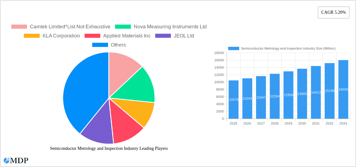
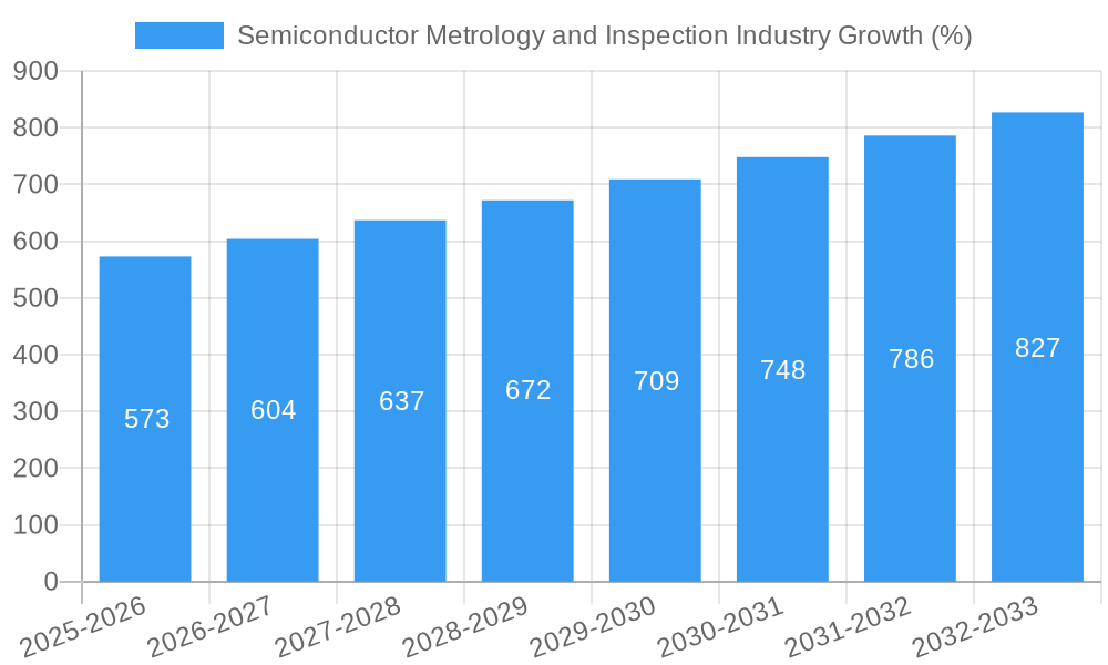
The semiconductor industry's relentless pursuit of miniaturization and performance enhancement fuels robust growth in the semiconductor metrology and inspection market. Driven by the increasing complexity of advanced semiconductor nodes (e.g., 5nm and beyond), the demand for precise and high-throughput metrology and inspection solutions is soaring. The market, currently valued at $10.47 billion (2025), is projected to experience a compound annual growth rate (CAGR) of 5.20% from 2025 to 2033, reaching an estimated value exceeding $16 billion by 2033. This expansion is propelled by factors such as the rising adoption of advanced packaging technologies, the growth of the 5G and IoT markets, and the increasing need for quality control throughout the manufacturing process. Key segments driving this growth include lithography metrology, which ensures the precise patterning of circuits, and wafer inspection, crucial for identifying defects early in the manufacturing process. The market’s expansion is further stimulated by continuous advancements in technology, leading to improved resolution, speed, and automation in metrology and inspection tools.
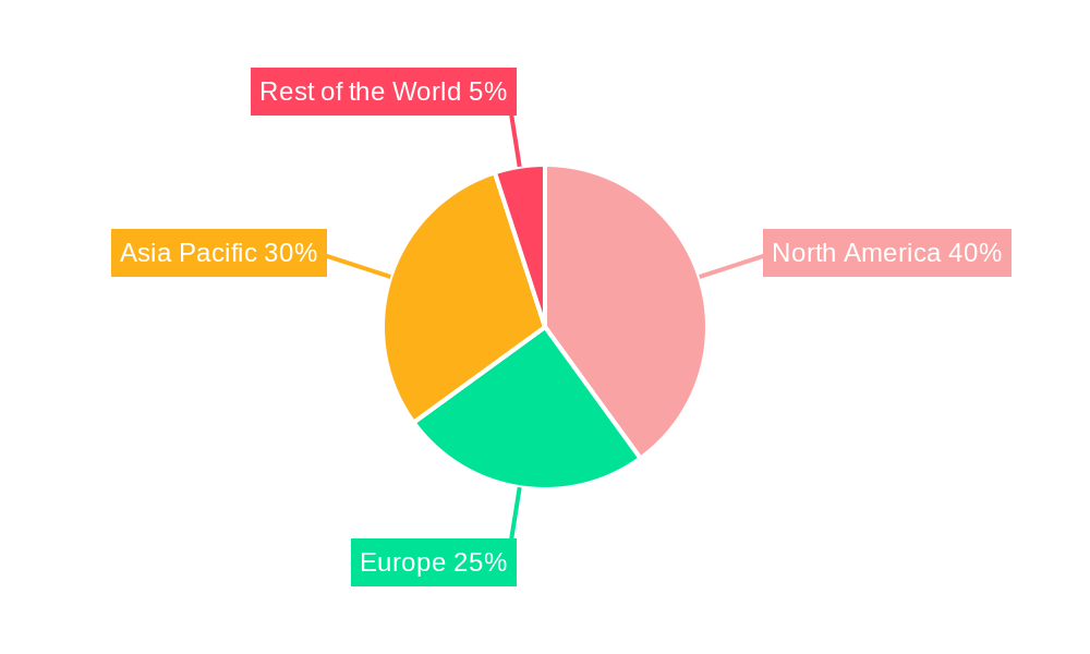
Competition in the market is fierce, with major players like KLA Corporation, Applied Materials, and ASML holding significant market share. However, innovative startups and smaller companies are also emerging, offering specialized solutions and challenging established players. Geographic distribution shows a strong concentration in North America and Asia-Pacific, reflecting the high density of semiconductor manufacturing facilities in these regions. While Europe and the rest of the world contribute significantly, these regions are expected to witness comparatively slower growth compared to the leading regions. The continuous need for higher accuracy and faster processing speeds is expected to drive further innovation, leading to the emergence of new technologies and the consolidation of existing players in the coming years. The increasing focus on sustainability and reduced manufacturing costs will also influence the future trajectory of the market.
Semiconductor Metrology and Inspection Market Report: 2019-2033 Forecast
Unlocking the Future of Semiconductor Manufacturing: A Comprehensive Analysis of the $XX Billion Metrology and Inspection Market
This in-depth report provides a comprehensive analysis of the global Semiconductor Metrology and Inspection market, offering invaluable insights for stakeholders across the value chain. Based on extensive research spanning the period 2019-2033 (Study Period), with 2025 as the Base and Estimated Year, and a forecast period of 2025-2033 (Forecast Period) and a historical period of 2019-2024 (Historical Period), this report delivers actionable intelligence to navigate the complexities of this rapidly evolving landscape. The market is projected to reach $XX Billion by 2033.
Semiconductor Metrology and Inspection Industry Market Dynamics & Concentration
The semiconductor metrology and inspection market is characterized by a moderately concentrated landscape, with key players vying for market share. The market's dynamics are driven by continuous innovation, stringent regulatory frameworks governing semiconductor production, and the emergence of substitute technologies. End-user demand, primarily from the booming electronics and automotive sectors, significantly influences market growth. Furthermore, strategic mergers and acquisitions (M&A) are reshaping the competitive dynamics. In the period 2019-2024, we witnessed approximately XX M&A deals, resulting in a market share consolidation among the leading players. Key factors influencing market concentration include:
- Technological Innovation: The constant drive for miniaturization and improved chip performance fuels demand for advanced metrology and inspection tools.
- Stringent Regulatory Compliance: Growing emphasis on quality control and safety necessitates sophisticated inspection techniques.
- Product Substitution: The emergence of alternative inspection technologies presents both opportunities and threats.
- End-User Trends: The growing adoption of 5G, AI, and IoT fuels demand for higher-performance chips and, consequently, more advanced inspection equipment.
- Consolidation through M&A: Strategic acquisitions and mergers are leading to larger entities with a broader portfolio of products and services. This trend is expected to continue in the coming years. For example, [Insert a relevant M&A deal example if available].
Semiconductor Metrology and Inspection Industry Industry Trends & Analysis
The semiconductor metrology and inspection market is experiencing robust growth, driven by several key factors. The Compound Annual Growth Rate (CAGR) during the forecast period (2025-2033) is estimated to be XX%, propelled by:
- Increasing demand for advanced semiconductor devices: The growing adoption of smartphones, wearables, and other electronic devices fuels the need for more sophisticated chips, necessitating precise metrology and inspection. Market penetration of advanced nodes (e.g., 5nm, 3nm) continues to increase.
- Technological advancements: Continuous innovation in metrology technologies, such as AI-powered defect detection and advanced optical techniques, are enhancing accuracy and efficiency.
- Stringent quality control requirements: The demand for higher yield and reduced defect rates in semiconductor manufacturing underscores the importance of robust inspection processes.
- Growing investments in R&D: Major players are heavily investing in R&D to develop next-generation metrology and inspection technologies, further driving market growth.
- Increased adoption of advanced packaging technologies: The growing complexity of semiconductor packaging demands sophisticated inspection techniques to ensure reliable interconnections.
This growth, however, is influenced by competitive dynamics, with major players constantly innovating to maintain a leading position.
Leading Markets & Segments in Semiconductor Metrology and Inspection Industry
The Asia-Pacific region, particularly Taiwan and South Korea, dominates the semiconductor metrology and inspection market, driven by the high concentration of semiconductor manufacturing facilities. Significant growth is also expected from other regions, including North America and Europe. Among the various segments, wafer inspection currently holds the largest market share due to the high volume of wafer fabrication.
Key Drivers by Segment:
- Lithography Metrology: Driven by the increasing complexity of lithographic processes and the need for precise overlay and critical dimension measurements.
- Mask Inspection and Metrology: Fueled by the increasing demand for high-resolution masks for advanced chip manufacturing.
- Wafer Inspection: Driven by the need for high-throughput and high-accuracy defect detection in wafer fabrication.
- Thin Film Metrology: Fueled by the increasing adoption of advanced thin film materials in semiconductor devices.
- Other Process Control Systems: Growth is driven by the increasing need for integrated process control solutions to optimize semiconductor manufacturing.
Regional Dominance:
- Asia-Pacific: Strong government support for the semiconductor industry, coupled with substantial investments in advanced manufacturing facilities, makes this region the primary market driver. Specific countries like Taiwan and South Korea benefit from strong government policies and advanced infrastructure.
- North America: High R&D expenditure and the presence of major equipment manufacturers contribute to significant market share.
- Europe: While a smaller market compared to Asia-Pacific, Europe is experiencing steady growth due to increasing investments in semiconductor manufacturing and R&D.
Semiconductor Metrology and Inspection Industry Product Developments
Recent product innovations focus on higher throughput, improved resolution, and enhanced automation. Artificial intelligence (AI) and machine learning (ML) are increasingly integrated into metrology systems for advanced defect detection and analysis. These advancements enhance productivity, reduce inspection time, and improve the overall accuracy of semiconductor manufacturing processes, leading to higher yields and lower costs. The market is witnessing the emergence of multi-functional metrology systems, integrating various inspection techniques into a single platform, to increase efficiency.
Key Drivers of Semiconductor Metrology and Inspection Industry Growth
Several factors contribute to the growth of the semiconductor metrology and inspection market. These include:
- Technological advancements: Continuous innovation in semiconductor technology necessitates equally advanced metrology tools for precise measurements and defect detection.
- Increasing demand for advanced semiconductor devices: The rising adoption of electronics across various industries drives demand for higher-performing chips.
- Government support and incentives: Governments worldwide are investing heavily in the semiconductor industry, promoting growth in related sectors, including metrology.
Challenges in the Semiconductor Metrology and Inspection Industry Market
The semiconductor metrology and inspection market faces several challenges:
- High capital expenditure: Advanced metrology systems are expensive, limiting access for smaller companies.
- Supply chain disruptions: Global supply chain volatility can impact the availability of critical components, affecting production and delivery timelines.
- Intense competition: The market is highly competitive, with established players and new entrants constantly vying for market share.
Emerging Opportunities in Semiconductor Metrology and Inspection Industry
The long-term growth of this market is driven by opportunities such as:
- Expanding applications of AI and ML: Integrating AI and ML into metrology systems enhances accuracy and efficiency.
- Growth of the 3D NAND and advanced packaging markets: These high-growth segments require specialized metrology solutions, opening up new opportunities.
- Increased demand for advanced process control: Advanced metrology data can optimize semiconductor manufacturing processes, improving yield and reducing costs.
Leading Players in the Semiconductor Metrology and Inspection Industry Sector
- Camtek Limited
- Nova Measuring Instruments Ltd
- KLA Corporation
- Applied Materials Inc
- JEOL Ltd
- Hitachi Hi-Technologies Corporation (Hitachi Limited)
- Lasertec Corporation
- Nikon Metrology NV (Nikon Group)
- Thermo Fisher Scientific Inc
- Onto Innovation Inc
- ASML Holding NV
Key Milestones in Semiconductor Metrology and Inspection Industry Industry
- 2020: Introduction of AI-powered defect detection software by [Company Name - replace with an example if available].
- 2021: Launch of a new high-resolution inspection system by [Company Name - replace with an example if available].
- 2022: Acquisition of [Company A] by [Company B] - replace with an example if available.
- 2023: [Add another significant milestone with year and brief description]
- 2024: [Add another significant milestone with year and brief description]
Strategic Outlook for Semiconductor Metrology and Inspection Industry Market
The future of the semiconductor metrology and inspection market is bright, with continued growth driven by technological advancements, increasing demand for advanced semiconductor devices, and government support for the semiconductor industry. Strategic partnerships, investments in R&D, and expansion into new markets will be crucial for success in this dynamic landscape. The market is poised for further consolidation, with leading players expected to expand their portfolios through M&A activities and strategic alliances. The focus on innovative solutions, leveraging AI and ML, will be a key differentiator for sustained growth and market leadership.
Semiconductor Metrology and Inspection Industry Segmentation
-
1. Type
-
1.1. Lithography Metrology
- 1.1.1. Overlay
- 1.1.2. Dimension Equipment
- 1.1.3. Mask Inspection and Metrology
- 1.2. Wafer Inspection
- 1.3. Thin Film Metrology
- 1.4. Other Process Control Systems
-
1.1. Lithography Metrology
Semiconductor Metrology and Inspection Industry Segmentation By Geography
- 1. North America
- 2. Europe
- 3. Asia Pacific
- 4. Rest of the World
Semiconductor Metrology and Inspection Industry REPORT HIGHLIGHTS
| Aspects | Details |
|---|---|
| Study Period | 2019-2033 |
| Base Year | 2024 |
| Estimated Year | 2025 |
| Forecast Period | 2025-2033 |
| Historical Period | 2019-2024 |
| Growth Rate | CAGR of 5.20% from 2019-2033 |
| Segmentation |
|
Table of Contents
- 1. Introduction
- 1.1. Research Scope
- 1.2. Market Segmentation
- 1.3. Research Methodology
- 1.4. Definitions and Assumptions
- 2. Executive Summary
- 2.1. Introduction
- 3. Market Dynamics
- 3.1. Introduction
- 3.2. Market Drivers
- 3.2.1 Increasing Demand for High-performance
- 3.2.2 Low-cost Semiconductors; Increasing Demand for Semiconductor Wafers in Consumer Electronics
- 3.3. Market Restrains
- 3.3.1. High Setup Cost and Lack of Expertise in Handling Metrology Systems Efficiently; High Raw Material and Fabrication Costs
- 3.4. Market Trends
- 3.4.1. Wafer Inspection to Witness Significant Growth
- 4. Market Factor Analysis
- 4.1. Porters Five Forces
- 4.2. Supply/Value Chain
- 4.3. PESTEL analysis
- 4.4. Market Entropy
- 4.5. Patent/Trademark Analysis
- 5. Global Semiconductor Metrology and Inspection Industry Analysis, Insights and Forecast, 2019-2031
- 5.1. Market Analysis, Insights and Forecast - by Type
- 5.1.1. Lithography Metrology
- 5.1.1.1. Overlay
- 5.1.1.2. Dimension Equipment
- 5.1.1.3. Mask Inspection and Metrology
- 5.1.2. Wafer Inspection
- 5.1.3. Thin Film Metrology
- 5.1.4. Other Process Control Systems
- 5.1.1. Lithography Metrology
- 5.2. Market Analysis, Insights and Forecast - by Region
- 5.2.1. North America
- 5.2.2. Europe
- 5.2.3. Asia Pacific
- 5.2.4. Rest of the World
- 5.1. Market Analysis, Insights and Forecast - by Type
- 6. North America Semiconductor Metrology and Inspection Industry Analysis, Insights and Forecast, 2019-2031
- 6.1. Market Analysis, Insights and Forecast - by Type
- 6.1.1. Lithography Metrology
- 6.1.1.1. Overlay
- 6.1.1.2. Dimension Equipment
- 6.1.1.3. Mask Inspection and Metrology
- 6.1.2. Wafer Inspection
- 6.1.3. Thin Film Metrology
- 6.1.4. Other Process Control Systems
- 6.1.1. Lithography Metrology
- 6.1. Market Analysis, Insights and Forecast - by Type
- 7. Europe Semiconductor Metrology and Inspection Industry Analysis, Insights and Forecast, 2019-2031
- 7.1. Market Analysis, Insights and Forecast - by Type
- 7.1.1. Lithography Metrology
- 7.1.1.1. Overlay
- 7.1.1.2. Dimension Equipment
- 7.1.1.3. Mask Inspection and Metrology
- 7.1.2. Wafer Inspection
- 7.1.3. Thin Film Metrology
- 7.1.4. Other Process Control Systems
- 7.1.1. Lithography Metrology
- 7.1. Market Analysis, Insights and Forecast - by Type
- 8. Asia Pacific Semiconductor Metrology and Inspection Industry Analysis, Insights and Forecast, 2019-2031
- 8.1. Market Analysis, Insights and Forecast - by Type
- 8.1.1. Lithography Metrology
- 8.1.1.1. Overlay
- 8.1.1.2. Dimension Equipment
- 8.1.1.3. Mask Inspection and Metrology
- 8.1.2. Wafer Inspection
- 8.1.3. Thin Film Metrology
- 8.1.4. Other Process Control Systems
- 8.1.1. Lithography Metrology
- 8.1. Market Analysis, Insights and Forecast - by Type
- 9. Rest of the World Semiconductor Metrology and Inspection Industry Analysis, Insights and Forecast, 2019-2031
- 9.1. Market Analysis, Insights and Forecast - by Type
- 9.1.1. Lithography Metrology
- 9.1.1.1. Overlay
- 9.1.1.2. Dimension Equipment
- 9.1.1.3. Mask Inspection and Metrology
- 9.1.2. Wafer Inspection
- 9.1.3. Thin Film Metrology
- 9.1.4. Other Process Control Systems
- 9.1.1. Lithography Metrology
- 9.1. Market Analysis, Insights and Forecast - by Type
- 10. North America Semiconductor Metrology and Inspection Industry Analysis, Insights and Forecast, 2019-2031
- 10.1. Market Analysis, Insights and Forecast - By Country/Sub-region
- 10.1.1.
- 11. Europe Semiconductor Metrology and Inspection Industry Analysis, Insights and Forecast, 2019-2031
- 11.1. Market Analysis, Insights and Forecast - By Country/Sub-region
- 11.1.1.
- 12. Asia Pacific Semiconductor Metrology and Inspection Industry Analysis, Insights and Forecast, 2019-2031
- 12.1. Market Analysis, Insights and Forecast - By Country/Sub-region
- 12.1.1.
- 13. Rest of the World Semiconductor Metrology and Inspection Industry Analysis, Insights and Forecast, 2019-2031
- 13.1. Market Analysis, Insights and Forecast - By Country/Sub-region
- 13.1.1.
- 14. Competitive Analysis
- 14.1. Global Market Share Analysis 2024
- 14.2. Company Profiles
- 14.2.1 Camtek Limited*List Not Exhaustive
- 14.2.1.1. Overview
- 14.2.1.2. Products
- 14.2.1.3. SWOT Analysis
- 14.2.1.4. Recent Developments
- 14.2.1.5. Financials (Based on Availability)
- 14.2.2 Nova Measuring Instruments Ltd
- 14.2.2.1. Overview
- 14.2.2.2. Products
- 14.2.2.3. SWOT Analysis
- 14.2.2.4. Recent Developments
- 14.2.2.5. Financials (Based on Availability)
- 14.2.3 KLA Corporation
- 14.2.3.1. Overview
- 14.2.3.2. Products
- 14.2.3.3. SWOT Analysis
- 14.2.3.4. Recent Developments
- 14.2.3.5. Financials (Based on Availability)
- 14.2.4 Applied Materials Inc
- 14.2.4.1. Overview
- 14.2.4.2. Products
- 14.2.4.3. SWOT Analysis
- 14.2.4.4. Recent Developments
- 14.2.4.5. Financials (Based on Availability)
- 14.2.5 JEOL Ltd
- 14.2.5.1. Overview
- 14.2.5.2. Products
- 14.2.5.3. SWOT Analysis
- 14.2.5.4. Recent Developments
- 14.2.5.5. Financials (Based on Availability)
- 14.2.6 Hitachi Hi-Technologies Corporation (Hitachi Limited)
- 14.2.6.1. Overview
- 14.2.6.2. Products
- 14.2.6.3. SWOT Analysis
- 14.2.6.4. Recent Developments
- 14.2.6.5. Financials (Based on Availability)
- 14.2.7 Lasertec Corporation
- 14.2.7.1. Overview
- 14.2.7.2. Products
- 14.2.7.3. SWOT Analysis
- 14.2.7.4. Recent Developments
- 14.2.7.5. Financials (Based on Availability)
- 14.2.8 Nikon Metrology NV (Nikon Group)
- 14.2.8.1. Overview
- 14.2.8.2. Products
- 14.2.8.3. SWOT Analysis
- 14.2.8.4. Recent Developments
- 14.2.8.5. Financials (Based on Availability)
- 14.2.9 Thermo Fisher Scientific Inc
- 14.2.9.1. Overview
- 14.2.9.2. Products
- 14.2.9.3. SWOT Analysis
- 14.2.9.4. Recent Developments
- 14.2.9.5. Financials (Based on Availability)
- 14.2.10 Onto Innovation Inc
- 14.2.10.1. Overview
- 14.2.10.2. Products
- 14.2.10.3. SWOT Analysis
- 14.2.10.4. Recent Developments
- 14.2.10.5. Financials (Based on Availability)
- 14.2.11 ASML Holding NV
- 14.2.11.1. Overview
- 14.2.11.2. Products
- 14.2.11.3. SWOT Analysis
- 14.2.11.4. Recent Developments
- 14.2.11.5. Financials (Based on Availability)
- 14.2.1 Camtek Limited*List Not Exhaustive
List of Figures
- Figure 1: Global Semiconductor Metrology and Inspection Industry Revenue Breakdown (Million, %) by Region 2024 & 2032
- Figure 2: North America Semiconductor Metrology and Inspection Industry Revenue (Million), by Country 2024 & 2032
- Figure 3: North America Semiconductor Metrology and Inspection Industry Revenue Share (%), by Country 2024 & 2032
- Figure 4: Europe Semiconductor Metrology and Inspection Industry Revenue (Million), by Country 2024 & 2032
- Figure 5: Europe Semiconductor Metrology and Inspection Industry Revenue Share (%), by Country 2024 & 2032
- Figure 6: Asia Pacific Semiconductor Metrology and Inspection Industry Revenue (Million), by Country 2024 & 2032
- Figure 7: Asia Pacific Semiconductor Metrology and Inspection Industry Revenue Share (%), by Country 2024 & 2032
- Figure 8: Rest of the World Semiconductor Metrology and Inspection Industry Revenue (Million), by Country 2024 & 2032
- Figure 9: Rest of the World Semiconductor Metrology and Inspection Industry Revenue Share (%), by Country 2024 & 2032
- Figure 10: North America Semiconductor Metrology and Inspection Industry Revenue (Million), by Type 2024 & 2032
- Figure 11: North America Semiconductor Metrology and Inspection Industry Revenue Share (%), by Type 2024 & 2032
- Figure 12: North America Semiconductor Metrology and Inspection Industry Revenue (Million), by Country 2024 & 2032
- Figure 13: North America Semiconductor Metrology and Inspection Industry Revenue Share (%), by Country 2024 & 2032
- Figure 14: Europe Semiconductor Metrology and Inspection Industry Revenue (Million), by Type 2024 & 2032
- Figure 15: Europe Semiconductor Metrology and Inspection Industry Revenue Share (%), by Type 2024 & 2032
- Figure 16: Europe Semiconductor Metrology and Inspection Industry Revenue (Million), by Country 2024 & 2032
- Figure 17: Europe Semiconductor Metrology and Inspection Industry Revenue Share (%), by Country 2024 & 2032
- Figure 18: Asia Pacific Semiconductor Metrology and Inspection Industry Revenue (Million), by Type 2024 & 2032
- Figure 19: Asia Pacific Semiconductor Metrology and Inspection Industry Revenue Share (%), by Type 2024 & 2032
- Figure 20: Asia Pacific Semiconductor Metrology and Inspection Industry Revenue (Million), by Country 2024 & 2032
- Figure 21: Asia Pacific Semiconductor Metrology and Inspection Industry Revenue Share (%), by Country 2024 & 2032
- Figure 22: Rest of the World Semiconductor Metrology and Inspection Industry Revenue (Million), by Type 2024 & 2032
- Figure 23: Rest of the World Semiconductor Metrology and Inspection Industry Revenue Share (%), by Type 2024 & 2032
- Figure 24: Rest of the World Semiconductor Metrology and Inspection Industry Revenue (Million), by Country 2024 & 2032
- Figure 25: Rest of the World Semiconductor Metrology and Inspection Industry Revenue Share (%), by Country 2024 & 2032
List of Tables
- Table 1: Global Semiconductor Metrology and Inspection Industry Revenue Million Forecast, by Region 2019 & 2032
- Table 2: Global Semiconductor Metrology and Inspection Industry Revenue Million Forecast, by Type 2019 & 2032
- Table 3: Global Semiconductor Metrology and Inspection Industry Revenue Million Forecast, by Region 2019 & 2032
- Table 4: Global Semiconductor Metrology and Inspection Industry Revenue Million Forecast, by Country 2019 & 2032
- Table 5: Semiconductor Metrology and Inspection Industry Revenue (Million) Forecast, by Application 2019 & 2032
- Table 6: Global Semiconductor Metrology and Inspection Industry Revenue Million Forecast, by Country 2019 & 2032
- Table 7: Semiconductor Metrology and Inspection Industry Revenue (Million) Forecast, by Application 2019 & 2032
- Table 8: Global Semiconductor Metrology and Inspection Industry Revenue Million Forecast, by Country 2019 & 2032
- Table 9: Semiconductor Metrology and Inspection Industry Revenue (Million) Forecast, by Application 2019 & 2032
- Table 10: Global Semiconductor Metrology and Inspection Industry Revenue Million Forecast, by Country 2019 & 2032
- Table 11: Semiconductor Metrology and Inspection Industry Revenue (Million) Forecast, by Application 2019 & 2032
- Table 12: Global Semiconductor Metrology and Inspection Industry Revenue Million Forecast, by Type 2019 & 2032
- Table 13: Global Semiconductor Metrology and Inspection Industry Revenue Million Forecast, by Country 2019 & 2032
- Table 14: Global Semiconductor Metrology and Inspection Industry Revenue Million Forecast, by Type 2019 & 2032
- Table 15: Global Semiconductor Metrology and Inspection Industry Revenue Million Forecast, by Country 2019 & 2032
- Table 16: Global Semiconductor Metrology and Inspection Industry Revenue Million Forecast, by Type 2019 & 2032
- Table 17: Global Semiconductor Metrology and Inspection Industry Revenue Million Forecast, by Country 2019 & 2032
- Table 18: Global Semiconductor Metrology and Inspection Industry Revenue Million Forecast, by Type 2019 & 2032
- Table 19: Global Semiconductor Metrology and Inspection Industry Revenue Million Forecast, by Country 2019 & 2032
Frequently Asked Questions
1. What is the projected Compound Annual Growth Rate (CAGR) of the Semiconductor Metrology and Inspection Industry?
The projected CAGR is approximately 5.20%.
2. Which companies are prominent players in the Semiconductor Metrology and Inspection Industry?
Key companies in the market include Camtek Limited*List Not Exhaustive, Nova Measuring Instruments Ltd, KLA Corporation, Applied Materials Inc, JEOL Ltd, Hitachi Hi-Technologies Corporation (Hitachi Limited), Lasertec Corporation, Nikon Metrology NV (Nikon Group), Thermo Fisher Scientific Inc, Onto Innovation Inc, ASML Holding NV.
3. What are the main segments of the Semiconductor Metrology and Inspection Industry?
The market segments include Type.
4. Can you provide details about the market size?
The market size is estimated to be USD 10.47 Million as of 2022.
5. What are some drivers contributing to market growth?
Increasing Demand for High-performance. Low-cost Semiconductors; Increasing Demand for Semiconductor Wafers in Consumer Electronics.
6. What are the notable trends driving market growth?
Wafer Inspection to Witness Significant Growth.
7. Are there any restraints impacting market growth?
High Setup Cost and Lack of Expertise in Handling Metrology Systems Efficiently; High Raw Material and Fabrication Costs.
8. Can you provide examples of recent developments in the market?
N/A
9. What pricing options are available for accessing the report?
Pricing options include single-user, multi-user, and enterprise licenses priced at USD 4750, USD 5250, and USD 8750 respectively.
10. Is the market size provided in terms of value or volume?
The market size is provided in terms of value, measured in Million.
11. Are there any specific market keywords associated with the report?
Yes, the market keyword associated with the report is "Semiconductor Metrology and Inspection Industry," which aids in identifying and referencing the specific market segment covered.
12. How do I determine which pricing option suits my needs best?
The pricing options vary based on user requirements and access needs. Individual users may opt for single-user licenses, while businesses requiring broader access may choose multi-user or enterprise licenses for cost-effective access to the report.
13. Are there any additional resources or data provided in the Semiconductor Metrology and Inspection Industry report?
While the report offers comprehensive insights, it's advisable to review the specific contents or supplementary materials provided to ascertain if additional resources or data are available.
14. How can I stay updated on further developments or reports in the Semiconductor Metrology and Inspection Industry?
To stay informed about further developments, trends, and reports in the Semiconductor Metrology and Inspection Industry, consider subscribing to industry newsletters, following relevant companies and organizations, or regularly checking reputable industry news sources and publications.
Methodology
Step 1 - Identification of Relevant Samples Size from Population Database


Step 2 - Approaches for Defining Global Market Size (Value, Volume* & Price*)

Note*: In applicable scenarios
Step 3 - Data Sources
Primary Research
- Web Analytics
- Survey Reports
- Research Institute
- Latest Research Reports
- Opinion Leaders
Secondary Research
- Annual Reports
- White Paper
- Latest Press Release
- Industry Association
- Paid Database
- Investor Presentations

Step 4 - Data Triangulation
Involves using different sources of information in order to increase the validity of a study
These sources are likely to be stakeholders in a program - participants, other researchers, program staff, other community members, and so on.
Then we put all data in single framework & apply various statistical tools to find out the dynamic on the market.
During the analysis stage, feedback from the stakeholder groups would be compared to determine areas of agreement as well as areas of divergence
